Mysterious seismic wave speed-up deep within Earth’s mantle explained at last
Scientists in Switzerland and Japan have uncovered what they say is the first direct evidence that materials at the bottom of the Earth’s mantle flow like a massive river. This literally “ground-breaking” finding, made by comparing seismic data with laboratory studies of materials at high pressures and temperatures, could reshape our understanding of the dynamics at play deep within our planet’s interior.
For over half a century, one of the greatest unresolved mysteries in geosciences has been a phenomenon that occurs just above the boundary where the Earth’s solid mantle meets its liquid core, says Motohiko Murakami, a geophysicist at ETH Zurich who led the new research effort. Within this so-called D” layer, the velocity of seismic waves passing through the mantle abruptly increases, and no-one is entirely sure why.
This increase is known as the D” discontinuity, and one possible explanation for it is a change in the material the waves are travelling through. Indeed, in 2004, Murakami and colleagues at the Tokyo Institute of Technology’s department of earth and planetary sciences suspected they’d uncovered an explanation along just these lines.
In this earlier study, the researchers showed that perovskite – the main mineral present in the Earth’s lower mantle – transforms into a different substance known as post-perovskite under the extreme pressures and temperatures characteristic of the D” layer. Accordingly, they hypothesized that this phase change could explain the jump in the speed of seismic waves.
Nature, however, had other ideas. “In an experimental study on seismic wave speeds across the post-perovskite phase transition we conducted three years later, such a sharp increase in velocity was not observed, bringing the problem back to square one,” Murakami says.
Post-perovskite crystals line up
Subsequent computer modelling revealed a subtler effect at play. According to these models, the hardness of post-perovskite materials is not fixed. Instead, it depends on the direction of the material’s crystals – and seismic waves through the material will only speed up when all the crystals point in the same direction.
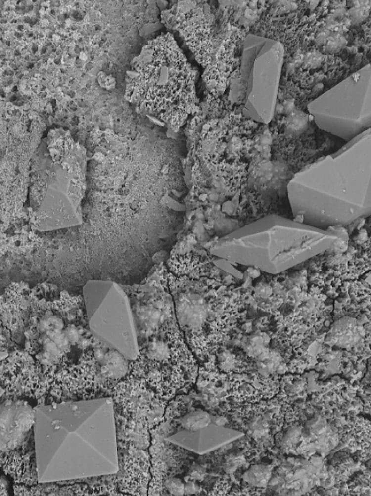
In the new work, which they detail in Communications Earth & Environment, Murakami and colleagues at Tohoku University and the Japan Synchrotron Radiation Research Institute confirmed this in a laboratory experiment for the first time. They obtained their results by placing crystals of a post-perovskite with the chemical formula MgGeO3 in a special apparatus designed to replicate the extreme pressures (around 1 million atmospheres) and temperatures (around 2500 K) found at the D” depth nearly 3000 km below the Earth’s surface. They then measured the velocity of lab-produced seismic waves sent through this material.
These measurements show that while randomly-oriented crystal samples do not reproduce the shear wave velocity jump at the D” discontinuity, crystals oriented along the (001) slip plane of the material’s lattice do. But what could make these crystals line up?
Evidence of a moving mantle
The answer, Murakami says, lies in slow, convective motions that cause the lower mantle to move at a rate of several centimetres per year. “This convection drives plate tectonics, volcanic activity and earthquakes but its effects have primarily been studied in the shallower region of the mantle,” he explains. “And until now, direct evidence of material movement in the deep mantle, nearly 3000 km beneath the surface, has remained elusive.”
Murakami explains that the post-perovskite mineral is rigid in one direction while being softer in others. “Since it naturally aligns its harder axis with the mantle flow, it effectively creates a structured arrangement at the base of the mantle,” he says.
According to Murakami, the discovery that solid (and not liquid) rock flows at this depth does more than just solve the D” layer mystery. It could also become a critical tool for identifying the locations at which large-scale mantle upwellings, or superplumes, originate. This, in turn, could provide new insights into Earth’s internal dynamics.
Building on these findings, the researchers say they now plan to further investigate the causes of superplume formation. “Superplumes are believed to trigger massive volcanic eruptions at the Earth’s surface, and their activity has shown a striking correlation — occurring just before two major mass extinction events in Earth’s history,” Murakami says.
Being able to understand – and perhaps even predict – future superplume activity could therefore “provide critical insights into the long-term survival of humanity”, he tells Physics World. “Such deep mantle processes may have profound implications for global environmental stability,” he says. “By advancing this research, we aim to uncover the mechanisms driving these extraordinary mantle events and assess their potential impact on Earth’s future.”
The post Mysterious seismic wave speed-up deep within Earth’s mantle explained at last appeared first on Physics World.