In this episode of Space Minds, host Mike Gruss sits down with Matt Magaña, President of Space, Defense & National Security at Voyager Technologies, to explore one of the most consequential national security space stories of 2025: Golden Dome.
LENEXA, KS – Enduralock is pleased to announce the successful completion of form, fit, and function testing for its OneLink™ satellite docking connector in Arkisys’ 1G robotic ground test facility […]
For years, both the Trump Administration and Congress have clearly stated that returning Americans to the moon before China in the 2028-2030 timeframe is a national priority. It is central to United States leadership in space, to global influence and to the future of human exploration. Yet across the space community, a sobering recognition has […]
Physics World is delighted to announce its Top 10 Breakthroughs of the Year for 2025, which includes research in astronomy, antimatter, atomic and molecular physics and more. The Top Ten is the shortlist for the Physics World Breakthrough of the Year, which will be revealed on Thursday 18 December.
Our editorial team has looked back at all the scientific discoveries we have reported on since 1 January and has picked 10 that we think are the most important. In addition to being reported in Physics World in 2025, the breakthroughs must meet the following criteria:
Significant advance in knowledge or understanding
Importance of work for scientific progress and/or development of real-world applications
Of general interest to Physics World readers
Here, then, are the Physics World Top 10 Breakthroughs for 2025, listed in no particular order. You can listen to Physics World editors make the case for each of our nominees in the Physics World Weekly podcast. And, come back next week to discover who has bagged the 2025 Breakthrough of the Year.
Analysing returned samples Tim McCoy (right), curator of meteorites at the Smithsonian’s National Museum of Natural History, and research geologist Cari Corrigan examine scanning electron microscope (SEM) images of a Bennu sample. (Courtesy: James Di Loreto, Smithsonian)
To Tim McCoy, Danny Glavin, Jason Dworkin, Yoshihiro Furukawa, Ann Nguyen, Scott Sandford, Zack Gainsforth and an international team of collaborators for identifying salt, ammonia, sugar, nitrogen- and oxygen-rich organic materials, and traces of metal-rich supernova dust, in samples returned from the near-Earth asteroid 101955 Bennu. The incredible chemical richness of this asteroid, which NASA’s OSIRIS-REx spacecraft visited in 2020, lends support to the longstanding hypothesis that asteroid impacts could have “seeded” the early Earth with the raw ingredients needed for life to form. The discoveries also enhance our understanding of how Bennu and other objects in the solar system formed out of the disc of material that coalesced around the young Sun.
To Takamasa Momose of the University of British Columbia, Canada, and Susumu Kuma of the RIKEN Atomic, Molecular and Optical Physics Laboratory, Japan for observing superfluidity in a molecule for the first time. Molecular hydrogen is the simplest and lightest of all molecules, and theorists predicted that it would enter a superfluid state at a temperature between 1‒2 K. But this is well below the molecule’s freezing point of 13.8 K, so Momose, Kuma and colleagues first had to develop a way to keep the hydrogen in a liquid state. Once they did that, they then had to work out how to detect the onset of superfluidity. It took them nearly 20 years, but by confining clusters of hydrogen molecules inside helium nanodroplets, embedding a methane molecule within the clusters, and monitoring the methane’s rotation, they were finally able to do it. They now plan to study larger clusters of hydrogen, with the aim of exploring the boundary between classical and quantum behaviour in this system.
To researchers at the University of Southampton and Microsoft Azure Fiber in the UK, for developing a new type of optical fibre that reduces signal loss, boosts bandwidth and promises faster, greener communications. The team, led by Francesco Poletti, achieved this feat by replacing the glass core of a conventional fibre with air and using glass membranes that reflect light at certain frequencies back into the core to trap the light and keep it moving through the fibre’s hollow centre. Their results show that the hollow-core fibres exhibit 35% less attenuation than standard glass fibres – implying that fewer amplifiers would be needed in long cables – and increase transmission speeds by 45%. Microsoft has begun testing the new fibres in real systems, installing segments in its network and sending live traffic through them. These trials open the door to gradual rollout and Poletti suggests that the hollow-core fibres could one day replace existing undersea cables.
PAT pioneers The research team in the proton therapy gantry room. (Courtesy: UO Fisica Sanitaria and UO Protonterapia, APSS, Trento)
To Francesco Fracchiolla and colleagues at the Trento Proton Therapy Centre in Italy for delivering the first clinical treatments using proton arc therapy (PAT). Proton therapy – a precision cancer treatment – is usually performed using pencil-beam scanning to precisely paint the dose onto the tumour. But this approach can be limited by the small number of beam directions deliverable in an acceptable treatment time. PAT overcomes this by moving to an arc trajectory with protons delivered over a large number of beam angles and the potential to optimize the number of energies used for each beam direction. Working with researchers at RaySearch Laboratories in Sweden, the team performed successful dosimetric comparisons with clinical proton therapy plans. Following a feasibility test that confirmed the viability of clinical PAT delivery, the researchers used PAT to treat nine cancer patients. Importantly, all treatments were performed using the centre’s existing proton therapy system and clinical workflow.
To Peter Maurer and David Awschalom at the University of Chicago Pritzker School of Molecular Engineering and colleagues for designing a protein quantum bit (qubit) that can be produced directly inside living cells and used as a magnetic field sensor. While many of today’s quantum sensors are based on nitrogen–vacancy (NV) centres in diamond, they are large and hard to position inside living cells. Instead, the team used fluorescent proteins, which are just 3 nm in diameter and can be produced by cells at a desired location with atomic precision. These proteins possess similar optical and spin properties to those of NV centre-based qubits – namely that they have a metastable triplet state. The researchers used a near-infrared laser pulse to optically address a yellow fluorescent protein and read out its triplet spin state with up to 20% spin contrast. They then genetically modified the protein to be expressed in bacterial cells and measured signals with a contrast of up to 8%. They note that although this performance does not match that of NV quantum sensors, it could enable magnetic resonance measurements directly inside living cells, which NV centres cannot do.
To Guangyu Zhang, Luojun Du and colleagues at the Institute of Physics of the Chinese Academy of Sciences for producing the first 2D sheets of metal. Since the discovery of graphene – a sheet of carbon just one atom thick – in 2004, hundreds of other 2D materials have been fabricated and studied. In most of these, layers of covalently bonded atoms are separated by gaps where neighbouring layers are held together only by weak van der Waals (vdW) interactions, making it relatively easy to “shave off” single layers to make 2D sheets. Many thought that making atomically thin metals, however, would be impossible given that each atom in a metal is strongly bonded to surrounding atoms in all directions. The technique developed by Zhang and Du and colleagues involves heating powders of pure metals between two monolayer-MoS2/sapphire vdW anvils. Once the metal powders are melted into a droplet, the researchers applied a pressure of 200 MPa and continued this “vdW squeezing” until the opposite sides of the anvils cooled to room temperature and 2D sheets of metal were formed. The team produced five atomically thin 2D metals – bismuth, tin, lead, indium and gallium – with the thinnest being around 6.3 Å. The researchers say their work is just the “tip of the iceberg” and now aim to study fundamental physics with the new materials.
Exquisite control Physicist Barbara Latacz at the BASE experiment at CERN. (Courtesy: CERN)
To CERN’s BASE collaboration for being the first to perform coherent spin spectroscopy on a single antiproton – the antimatter counterpart of the proton. Their breakthrough is the most precise measurement yet of the antiproton’s magnetic properties, and could be used to test the Standard Model of particle physics. The experiment begins with the creation of high-energy antiprotons in an accelerator. These must be cooled (slowed down) to cryogenic temperatures without being lost to annihilation. Then, a single antiproton is held in an ultracold electromagnetic trap, where microwave pulses manipulate its spin state. The resulting resonance peak was 16 times narrower than previous measurements, enabling a significant leap in precision. This level of quantum control opens the door to highly sensitive comparisons of the properties of matter (protons) and antimatter (antiprotons). Unexpected differences could point to new physics beyond the Standard Model and may also reveal why there is much more matter than antimatter in the visible universe.
To Richard Allen, director of the Berkeley Seismological Laboratory at the University of California, Berkeley, and Google’s Marc Stogaitis and colleagues for creating a global network of Android smartphones that acts as an earthquake early warning system. Traditional early warning systems use networks of seismic sensors that rapidly detect earthquakes in areas close to the epicentre and issue warnings across the affected region. Building such seismic networks, however, is expensive, and many earthquake-prone regions do not have them. The researchers utilized the accelerometer in millions of phones in 98 countries to create the Android Earthquake Alert (AEA) system. Testing the app between 2021 and 2024 led to the detection of an average of 312 earthquakes a month, with magnitudes ranging from 1.9 to 7.8. For earthquakes of magnitude 4.5 or higher, the system sent “TakeAction” alerts to users, sending them, on average, 60 times per month for an average of 18 million individual alerts per month. The system also delivered lesser “BeAware” alerts to regions expected to experience a shaking intensity of magnitude 3 or 4. The team now aims to produce maps of ground shaking, which could assist the emergency response services following an earthquake.
To Lisa Nortmann at Germany’s University of Göttingen and colleagues for creating the first detailed “weather map” of an exoplanet. The forecast for exoplanet WASP-127b is brutal with winds reaching 33,000 km/hr, which is much faster than winds found anywhere in the Solar System. The WASP-127b is a gas giant located about 520 light–years from Earth and the team used the CRIRES+ instrument on the European Southern Observatory’s Very Large Telescope to observe the exoplanet as it transited across its star in less than 7 h. Spectral analysis of the starlight that filtered through WASP-127b’s atmosphere revealed Doppler shifts caused by supersonic equatorial winds. By analysing the range of Doppler shifts, the team created a rough weather map of WASP-127b, even though they could not resolve light coming from specific locations on the exoplanet. Nortmann and colleagues concluded that the exoplanet’s poles are cooler that the rest of WASP-127b, where temperatures can exceed 1000 °C. Water vapour was detected in the atmosphere, raising the possibility of exotic forms of rain.
To the team led by Yichao Zhang at the University of Maryland and Pinshane Huang of the University of Illinois at Urbana-Champaign for capturing the highest-resolution images ever taken of individual atoms in a material. The team used an electron-microscopy technique called electron ptychography to achieve a resolution of 15 pm, which is about 10 times smaller than the size of an atom. They studied a stack of two atomically-thin layers of tungsten diselenide, which were rotated relative to each other to create a moiré superlattice. These twisted 2D materials are of great interest to physicists because their electronic properties can change dramatically with small changes in rotation angle. The extraordinary resolution of their microscope allowed them to visualize collective vibrations in the material called moiré phasons. These are similar to phonons, but had never been observed directly until now. The team’s observations align with theoretical predictions for moiré phasons. Their microscopy technique should boost our understanding of the role that moiré phasons and other lattice vibrations play in the physics of solids. This could lead to the engineering of new and useful materials.
Physics World‘s coverage of the Breakthrough of the Year is supported by Reports on Progress in Physics, which offers unparalleled visibility for your ground-breaking research.
This episode of the Physics World Weekly podcast features a lively discussion about our Top 10 Breakthroughs of 2025, which include important research in quantum sensing, planetary science, medical physics, 2D materials and more. Physics World editors explain why we have made our selections and look at the broader implications of this impressive body of research.
The top 10 serves as the shortlist for the Physics World Breakthrough of the Year award, the winner of which will be announced on 18 December.
Links to all the nominees, more about their research and the selection criteria can be found here.
Physics World‘s coverage of the Breakthrough of the Year is supported by Reports on Progress in Physics, which offers unparalleled visibility for your ground-breaking research.
The Sun regularly produces energetic outbursts of electromagnetic radiation called solar flares. When these flares are accompanied by flows of plasma, they are known as coronal mass ejections (CMEs). Now, astronomers at the Netherlands Institute for Radio Astronomy (ASTRON) have spotted a similar event occurring on a star other than our Sun – the first unambiguous detection of a CME outside our solar system.
Using these tools, the team detected short, intense radio signals from a star located around 40 light-years away from Earth. This star, called StKM 1-1262, is very different from our Sun. At only around half of the Sun’s mass, it is classed as an M-dwarf star. It also rotates 20 times faster and boasts a magnetic field 300 times stronger. Nevertheless, the burst it produced had the same frequency, time and polarization properties as the plasma emission from an event called a solar type II burst that astronomers identify as a fast CME when it comes from the Sun.
“This work opens up a new observational frontier for studying and understanding eruptions and space weather around other stars,” says Henrik Eklund, an ESA research fellow working at the European Space Research and Technology Centre (ESTEC) in Noordwijk, Netherlands, who was not involved in the study. “We’re no longer limited to extrapolating our understanding of the Sun’s CMEs to other stars.”
Implications for life on exoplanets
The high speed of this burst – around 2400 km/s – would be atypical for our own Sun, with only around 1 in every 20 solar CMEs reaching that level. However, the ASTRON team says that M-dwarfs like StKM 1-1262 could emit CMEs of this type as often as once a day.
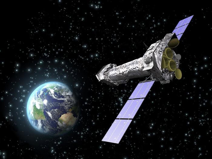
Spotting a distant coronal mass ejection: An artist’s impression of XMM-Newton. (Courtesy: ESA/C Carreau)
According to Eklund, this has implications for extraterrestrial life, as most of the known planets in the Milky Way are thought to orbit stars of this type, and such bursts could be powerful enough to strip their atmospheres. “It seems that intense space weather may be even more extreme around smaller stars – the primary hosts of potentially habitable exoplanets,” he says. “This has important implications for how these planets keep hold of their atmospheres and possibly remain habitable over time.”
Erik Kuulkers, a project scientist at XMM-Newton who was also not directly involved in the study, suggests that this atmosphere-stripping ability could modify the way we hunt for life in stellar systems akin to our Solar System. “A planet’s habitability for life as we know it is defined by its distance from its parent star – whether or not it sits within the star’s ‘habitable zone’, a region where liquid water can exist on the surface of planets with suitable atmospheres,” Kuulkers says. “What if that star was especially active, regularly producing CMEs, however? A planet regularly bombarded by these ejections might lose its atmosphere entirely, leaving behind a barren uninhabitable world, despite its orbit being ‘just right’.
Kuulkers adds that the study’s results also contain lessons for our own Solar System. “Why is there still life on Earth despite the violent material being thrown at us?” he asks. “It is because we are safeguarded by our atmosphere.”
Seeking more data
The ASTRON team’s next step will be to look for more stars like StKM 1-1262, which Kuulkers agrees is a good idea. “The more events we can find, the more we learn about CMEs and their impact on a star’s environment,” he says. Additional observations at other wavelengths “would help”, he adds, “but we have to admit that events like the strong one reported on in this work don’t happen too often, so we also need to be lucky enough to be looking at the right star at the right time.”
For now, the ASTRON researchers, who report their work in Nature, say they have reached the limit of what they can detect with LOFAR. “The next step is to use the next generation Square Kilometre Array, which will let us find many more such stars since it is so much more sensitive,” Callingham tells Physics World.
With support from Microsoft, Stripe, and Shopify, Running Tide billed itself as on the cutting edge of carbon removal. In the end, it resorted to dumping thousands of tons of wood chips in the sea.
NATO has picked 150 companies from 24 of its member countries to join its Defence Innovation Accelerator for the North Atlantic next year, including more than two dozen with ties to the space sector.
As on-orbit capabilities grow more advanced, ground systems are undergoing a transformation of their own. Ground network specialist ST Engineering iDirect, with headquarters in Herndon, Virginia, is investing in new […]