↩ Accueil

Vue normale

Il y a de nouveaux articles disponibles, cliquez pour rafraîchir la page.
À partir d’avant-hierPhysics World

New on-chip laser fills long sought-after green gap

26 septembre 2024 à 10:30
A series of visible-light colours generated by a microring resonator
Closing the green gap Series of visible-light colours generated by a microring resonator. (Courtesy: S Kelley/NIST)

On-chip lasers that emit green light are notoriously difficult to make. But researchers at the National Institute of Standards and Technology (NIST) and the NIST/University of Maryland Joint Quantum Institute may now have found a way to do just this, using a modified optical component known as a ring-shaped microresonator. Green lasers are important for applications including quantum sensing and computing, medicine and underwater communications.

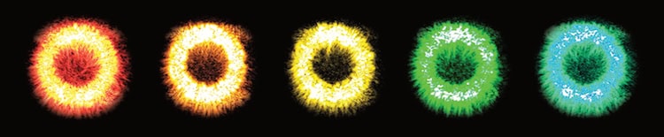
In the new work, a research team led by Kartik Srinivasan modified a silicon nitride microresonator such that it was able to convert infrared laser light into yellow and green light. The researchers had already succeeded in using this structure to convert infrared laser light into red, orange and yellow wavelengths, as well as a wavelength of 560 nm, which lies at the edge between yellow and green light. Previously, however, they were not able to produce the full range of yellow and green colours to fill the much sought-after “green gap”.

More than 150 distinct green-gap wavelengths

To overcome this problem, the researchers made two modifications to their resonator. The first was to thicken it by 100 nm so that it could more easily generate green light with wavelengths down to 532 nm. Being able to produce such a short wavelength means that the entire green wavelength range is now covered, they say. In parallel, they modified the cladding surrounding the microresonator by etching away part of the silicon dioxide layer that it was fabricated on. This alteration made the output colours less sensitive to the dimension of the microring.

These changes meant that the team could produce more than 150 distinct green-gap wavelengths and could fine tune these too. “Previously, we could make big changes – red to orange to yellow to green – in the laser colours we could generate with OPO [optical parametric oscillation], but it was hard to make small adjustments within each of these colour bands,” says Srinivasan.

Like the previous microresonator, the new device works thanks to a process known as nonlinear wave mixing. Here, infrared light that is pumped into the ring-shaped structure is confined and guided within it. “This infrared light circulates around the ring hundreds of times due to its low loss, resulting in a build-up of intensity,” explains Srinivasan. “This high intensity enables the conversion of pump light to other wavelengths.”

Third-order optical parametric oscillation

“The purpose of the microring is to enable relatively modest, input continuous-wave laser light to build up in intensity to the point that nonlinear optical effects, which are often thought of as weak, become very significant,” says team member Xiyuan Lu.

The specific nonlinear optical process the researchers use is third-order optical parametric oscillation. “This works by taking light at a pump frequency np and creating one beam of light that’s higher in frequency (called the signal, at a frequency ns) and one beam that’s lower in frequency (called the idler, at a frequency ni),” explains first author Yi Sun. “There is a basic energy conservation requirement that 2np= ns+ ni.”

Simply put, this means that for every two pump photons that are used to excite the system, one signal photon and one idler photon are created, he tells Physics World.

Towards higher power and a broader range of colours

The NIST/University of Maryland team has been working on optical parametric oscillation as a way to convert near-infrared laser light to visible laser light for several years now. One of their main objectives was to fill the green gap in laser technology and fabricate frequency-converted lasers for quantum, biology and display applications.

“Some of the major applications we are ultimately targeting are high-end lasers, continuous-wave single-mode lasers covering the green gap or even a wider range of frequencies,” reveals team member Jordan Stone. “Applications include lasers for quantum optics, biology and spectroscopy, and perhaps laser/hologram display technologies.”

For now, the researchers are focusing on achieving higher power and a broader range of colours (perhaps even down to blue wavelengths). They also hope to make devices that can be better controlled and tuned. “We are also interested in laser injection locking with frequency-converted lasers, or using other techniques to further enhance the coherence of our lasers,” says Stone.

The work is detailed in Light: Science & Applications.

The post New on-chip laser fills long sought-after green gap appeared first on Physics World.

  •  

Ambipolar electric field helps shape Earth’s ionosphere

25 septembre 2024 à 09:53

A drop in electric potential of just 0.55 V measured at altitudes of between 250–768 km in the Earth’s atmosphere above the North and South poles could be the first direct measurement of our planet’s long-sought after electrostatic field. The measurements, from NASA’s Endurance mission, reveal that this field is important for driving how ions escape into space and shaping the upper layer of the atmosphere, known as the ionosphere.

Researchers first predicted the existence of the ambipolar electric field in the 1960s as the first spacecraft flying over the Earth’s poles detected charged particles (including positively-charged hydrogen and oxygen ions) flowing out from the atmosphere. The theory of a planet-wide electric field was developed to directly explain this “polar wind”, but the effects of this field were thought to be too weak to be detectable. Indeed, if the ambipolar field was the only mechanism driving the electrostatic field of Earth, then the resulting electric potential drop across the exobase transition region (which lies at an altitude of between 200–780 km) could be as low as about 0.4 V.

A team of researchers led by Glyn Collinson at NASA’s Goddard Space Flight Center in Greenbelt, Maryland, has now succeeded in measuring this field for the first time thanks to a new instrument called a photoelectron spectrometer, which they developed. The device was mounted on the Endurance rocket, which was launched from Svalbard in the  Norwegian Arctic in May 2022. “Svalbard is the only rocket range in the world where you can fly through the polar wind and make the measurements we needed,” says team member Suzie Imber, who is a space physicist at the University of Leicester, UK.

Just the “right amount”

The spacecraft reached an altitude of 768.03 km, where it remained for 19 min while the onboard spectrometer measured the energies of electrons there every 10 seconds. It measured a drop in electric potential of 0.55 V±0.09 V over an altitude range of 258–769 km. While tiny, this is just the “right amount” to explain the polar wind without any other atmospheric effects, says Collinson.

The researchers showed that the ambipolar field, which is generated exclusively by the outward pressure of ionospheric electrons, increases the “scale height” of the ionosphere by as much as 271% (from a height of 77.0 km to a height of 208.9 km). This part of the atmosphere therefore remains denser to greater heights than it would if the field did not exist. This is because the field increases the supply of cold oxygen ions (O+) to the magnetosphere (that is, near the peak at 768 km) by more than 3.8%, so counteracting the effects of other mechanisms (such as wave-particle interactions) that can heat and accelerate these particles to velocities high enough for them to escape into space. The field also probably explains why the magnetosphere is made up primarily of cold hydrogen ions (H+).

The ambipolar field could be as fundamental for our planet as its gravity and magnetic fields, says Collinson, and it may even have helped shape how the atmosphere evolved. Similar fields might also exist on other planets in the solar system with an atmosphere, including Venus and Mars. “Understanding the forces that cause Earth’s atmosphere to slowly leak to space may be important for revealing what makes Earth habitable and why we’re all here,” he tells Physics World. “It’s also crucial to accurately forecast the impact of geomagnetic storms and ‘space weather’.”

Looking forward, the scientists say they would like to make further measurements of the Earth’s ambipolar field in the future. Happily, they recently received endorsement for a follow-up rocket – called Resolute – to do just this.

The post Ambipolar electric field helps shape Earth’s ionosphere appeared first on Physics World.

  •  

Light-absorbing dye turns skin of a live mouse transparent

24 septembre 2024 à 17:00

One of the difficulties when trying to image biological tissue using optical techniques is that tissue scatters light, which makes it opaque. This scattering occurs because the different components of tissue, such as water and lipids, have different refractive indices, and it limits the depth at which light can penetrate.

A team of researchers at Stanford University in the US has now found that a common water-soluble yellow dye (among several other dye molecules) that strongly absorbs near-ultraviolet and blue light can help make biological tissue transparent in just a few minutes, thus allowing light to penetrate more deeply. In tests on mice skin, muscle and connective tissue, the team used the technique to observe a wide range of deep-seated structures and biological activity.

In their work, the research team – led by Zihao Ou (now at The University of Texas at Dallas), Mark Brongersma and Guosong Hong – rubbed the common food dye tartrazine, which is yellow/red in colour, onto the abdomen, scalp and hindlimbs of live mice. By absorbing light in the blue part of the spectrum, the dye altered the refractive index of the water in the treated areas at red-light wavelengths, such that it more closely matched that of lipids in this part of the spectrum. This effectively reduced the refractive-index contrast between the water and the lipids and allowed the biological tissue to appear more transparent at this wavelength, albeit tinged with red.

In this way, the researchers were able to visualize internal organs, such as the liver, small intestine and bladder, through the skin without requiring any surgery. They were even able to observe fluorescent protein-labelled enteric neurons in the abdomen and monitor the movements of these nerve cells. This enabled them to generate maps showing different movement patterns in the gut during digestion. They were also able to visualize blood flow in the rodents’ brains and the fine structure of muscle sarcomere fibres in their hind limbs.

Reversible effect

The skin becomes transparent in just a few minutes and the effect can be reversed by simply rinsing off the dye.

So far, this “optical clearing” study has only been conducted on animals. But if extended to humans, it could offer a variety of benefits in biology, diagnostics and even cosmetics, says Hong. Indeed, the technique could help make some types of invasive biopsies a thing of the past.

“For example, doctors might be able to diagnose deep-seated tumours by simply examining a person’s tissue without the need for invasive surgical removal. It could potentially make blood draws less painful by helping phlebotomists easily locate veins under the skin and could also enhance procedures like laser tattoo removal by allowing more precise targeting of the pigment beneath the skin,” Hong explains. “If we could just look at what’s going on under the skin instead of cutting into it, or using radiation to get a less than clear look, we could change the way we see the human body.”

Hong tells Physics World that the collaboration originated from a casual conversation he had with Brongersma, at a café on Stanford’s campus during the summer of 2021. “Mark’s lab specializes in nanophotonics while my lab focuses on new strategies for enhancing deep-tissue imaging of neural activity and light delivery for optogenetics. At the time, one of my graduate students, Nick Rommelfanger (third author of the current paper), was working on applying the ‘Kramers-Kronig’ relations to investigate microwave–brain interactions. Meanwhile, my postdoc Zihao Ou (first author of this paper) had been systematically screening a variety of dye molecules to understand their interactions with light.”

Tartrazine emerged as the leading candidate, says Hong. “This dye showed intense absorption in the near-ultraviolet/blue spectrum (and thus strong enhancement of refractive index in the red spectrum), minimal absorption beyond 600 nm, high water solubility and excellent biocompatibility, as it is an FD&C-approved food dye.”

“We realized that the Kramers-Kronig relations could be applied to the resonance absorption of dye molecules, which led me to ask Mark about the feasibility of matching the refractive index in biological tissues, with the aim of reducing light scattering,” Hong explains. “Over the past three years, both our labs have had numerous productive discussions, with exciting results far exceeding our initial expectations.”

The researchers say they are now focusing on identifying other dye molecules with greater efficiency in achieving tissue transparency. “Additionally, we are exploring methods for cells to express intensely absorbing molecules endogenously, enabling genetically encoded tissue transparency in live animals,” reveals Hong.

The study is detailed in Science.

The post Light-absorbing dye turns skin of a live mouse transparent appeared first on Physics World.

  •  

Convection enhances heat transport in sea ice

24 septembre 2024 à 10:42

The thermal conductivity of sea ice can significantly increase when convective flow is present within the ice. This new result, from researchers at Macquarie University, Australia, and the University of Utah and Dartmouth College, both in the US, could allow for more accurate climate models – especially since current global models only account for temperature and salinity and not convective flow.

Around 15% of the ocean’s surface will be covered with sea ice at some time in a year. Sea ice is a thin layer that separates the atmosphere and the ocean and it is responsible for regulating heat exchange between the two in the polar regions of our planet. The thermal conductivity of sea ice is a key parameter in climate models. It has proved difficult to measure, however, because of its complex structure, made up of ice, air bubbles and brine inclusions, which form as the ice freezes from the surface of the ocean to deeper down. Indeed, sea ice can be thought of as being a porous composite material and is therefore very sensitive to changes in temperature and salinity.

The salty liquid within the brine inclusions is heavier than fresh ocean water. This results in convective flow within the ice, creating channels through which liquid can flow out, explains applied mathematician Noa Kraitzman at Macquarie, who led this new research effort. “Our new framework characterizes enhanced thermal transport in porous sea ice by combining advection-diffusion processes with homogenization theory, which simplifies complex physical properties into an effective bulk coefficient.”

Thermal conductivity of sea ice can increase by a factor of two to three

The new work builds on a 2001 study in which researchers observed an increase in thermal conductivity in sea ice at warmer temperatures. “In our calculations, we had to derive new bounds on the effective thermal conductivity, while also accounting for complex, two-dimensional convective fluid flow and developing a theoretical model that could be directly compared with experimental measurements in the field,” explains Kraitzman. “We employed Padé approximations to obtain the required bounds and parametrized the Péclet number specifically for sea ice, considering it as a saturated rock.”

Padé approximations are routinely used to approximate a function by a rational analysis of given order and the Péclet number is a dimensionless parameter defined as the ratio between the rate of advection to the rate of diffusion.

The results suggest that the effective thermal conductivity of sea ice can increase by a factor of two to three because of conductive flow, especially in the lower, warmer sections of the ice, where temperature and the ice’s permeability favour convection, Kraitzman tells Physics World. “This enhancement is mainly confined to the bottom 10 cm during the freezing season, when convective flows are present within the sea ice. Incorporating these bounds into global climate models could improve their ability to predict thermal transport through sea ice, resulting in more accurate predictions of sea ice melt rates.”

Looking forward, Kraitzman and colleagues say they now hope to acquire additional field measurements to refine and validate their model. They also want to extend their mathematical framework to include more general 3D flows and incorporate the complex fluid exchange processes that exist between ocean and sea ice. “By addressing these different areas, we aim to improve the accuracy and applicability of our model, particularly in ocean-sea ice interaction models, aiming for a better understanding of polar heat exchange processes and their global impacts,” says Kraitzman.

The present work is detailed in Proceedings of the Royal Society A.

The post Convection enhances heat transport in sea ice appeared first on Physics World.

  •  

Short-range order always appears in new type of alloy

23 septembre 2024 à 15:00

Short-range order plays an important role in defining the properties and performance of “multi-principal element alloys” (MPEAs), but the way in which this order develops is little understood, making it difficult to control. In a surprising new discovery, a US-based research collaboration has have found that this order exists regardless of how MPEAs are processed. The finding will help scientists develop more effective ways to improve the properties of these materials and even tune them for specific applications, especially those with demanding conditions.

MPEAs are a relatively new type of alloy and consist of three or more components in nearly equal proportions. This makes them very different to conventional alloys, which are made from just one or two principal elements with trace elements added to improve their performance.

In recent years, MPEAs have spurred a flurry of interest thanks to their high strength, hardness and toughness over temperature ranges at which traditional alloys, such as steel, can fail. They could also be more resistant to corrosion, making them promising for use in extreme conditions, such as in power plants, or aerospace and automotive technologies, to name but three.

Ubiquitous short-range order

MPEAs were originally thought of as being random solid solutions with the constituent elements being haphazardly dispersed, but recent experiments have shown that this is not the case.

The researchers – from Penn State University, the University of California, Irvine, the University of Massachusetts, Amherst, and Brookhaven National Laboratory – studied the cobalt/chromium/nickel (CoCrNi) alloy, one of the best-known examples of an MPEA. This face-centred cubic (FCC) alloy boasts the highest fracture toughness for an alloy at liquid helium temperatures ever recorded.

Using an improved transmission electron microscopy characterization technique combined with advanced three-dimensional printing and atomistic modelling, the team found that short-range order, which occurs when atoms are arranged in a non-random way over short distances, appears in three CoCrNi-based FCC MPEAs under a variety of processing and thermal treatment conditions.

Their computational modelling calculations also revealed that local chemical order forms in the liquid–solid interface when the alloys are rapidly cooled, even at a rate of 100 billion °C/s. This effect comes from the rapid atomic diffusion in the supercooled liquid, at rates equal to or even greater than the rate of solidification. Short-range order is therefore an inherent characteristic of FCC MPEAs, the researchers say.

The new findings are in contrast to the previous notion that the elements in MPEAs arrange themselves randomly in the crystal lattice if they cool rapidly during solidification. It also refutes the idea that short-range order develops mainly during annealing (a process in which heating and slow cooling are used to improve material properties such as strength, hardness and ductility).

Short-range order can affect MPEA properties, such as strength or resistance to radiation damage. The researchers, who report their work in Nature Communications, say they now plan to explore how corrosion and radiation damage affect the short-range order in MPEAs.

“MPEAs hold promise for structural applications in extreme environments. However, to facilitate their eventual use in industry, we need to have a more fundamental understanding of the structural origins that give rise to their superior properties,” says team co-lead Yang Yang, who works in the engineering science and mechanics department at Penn State.

The post Short-range order always appears in new type of alloy appeared first on Physics World.

  •  

Thermal dissipation decoheres qubits

23 septembre 2024 à 10:04

How does a Josephson junction, which is the basic component of a superconducting quantum bit (or qubit), release its energy into the environment? It is radiated as photons, according to new experiments by researchers at Aalto University Finland in collaboration with colleagues from Spain and the US who used a thermal radiation detector known as a bolometer to measure this radiation directly in the electrical circuits holding the qubits. The work will allow for a better understanding of the loss and decoherence mechanism in qubits that can disrupt and destroy quantum information, they say.

Quantum computers make use of qubits to store and process information. The most advanced quantum computers to date – including those being developed by IT giants Google and IBM – use qubits made from superconducting electronic circuits operating at very low temperatures. To further improve qubits, researchers need to better understand how they dissipate heat, says Bayan Karimi, who is the first author of a paper describing the new study. This heat transfer is a form of decoherence – a phenomenon by which the quantum states in qubits revert to behaving like classical 0s and 1s and lose the precious quantum information they contain.

“An understanding of dissipation in a single Josephson junction coupled to an environment remains strikingly incomplete, however,” she explains. “Today, a junction can be modelled and characterized without a detailed knowledge of, for instance, where energy is dissipated in a circuit. But improving design and performance will require a more complete picture.”

Physical environment is important

In the new work, Karimi and colleagues used a nano-bolometer to measure the very weak radiation emitted from a Josephson junction over a broad range of frequencies up to 100::GHz. The researchers identified several operation regimes depending on the junction bias, each with a dominant dissipation mechanism. “The whole frequency-dependent power and shape of the current-voltage characteristics can be attributed to the physical environment of the junction,” says Jukka Pekola, who led this new research effort.

The thermal detector works by converting radiation into heat and is composed of an absorber (made of copper), the temperature of which changes when it detects the radiation. The researchers measure this variation using a sensitive thermometer, comprising a tunnel junction between the copper absorber and a superconductor.

“Our work will help us better understand the nature of heat dissipation of qubits that can disrupt and destroy quantum information and how these coherence losses can be directly measured as thermal losses in the electrical circuit holding the qubits,” Karimi tells Physics World.

In the current study, which is detailed in Nature Nanotechnology, the researchers say they measured continuous energy release from a Josephson junction when it was biased by a voltage. They now aim to find out how their detector can sense single heat loss events when the Josephson junction or qubit releases energy. “At best, we will be able to count single photons,” says Pekola.

The post Thermal dissipation decoheres qubits appeared first on Physics World.

  •  

New superconductor has record breaking current density

17 septembre 2024 à 12:28

A superconducting wire segment based on rare-earth barium copper oxide (REBCO) is the highest performing yet in terms of current density, carrying 190 MA/cm2 in the absence of any external magnetic field at a temperature of 4.2 K. At warmer temperatures of 20 K (which is the proposed application temperature for magnets used in commercial nuclear fusion reactors), the wires can still carry over 150 MA/cm2. These figures mean that the wire, despite being only 0.2 micron thick, can carry a current comparable to that of commercial superconducting wires that are almost 10 times thicker, according to its developers at the University at Buffalo in the US.

High-temperature superconducting (HTS) wires could be employed in a host of applications, including energy generation, storage and transmission, transportation, and in the defence and medical sectors. They might also be used in commercial nuclear fusion, offering the possibility of limitless clean energy. Indeed, if successful, this niche application could help address the world’s energy supply issues, says Amit Goyal of the University at Buffalo’s School of Engineering and Applied Science, who co-led this new study.

Record-breaking critical current density and pinning force

Before such large-scale applications see the light of day, however, the performance of HTS wires must be improved – and their cost reduced. Goyal and colleagues’ new HTS wire has the highest values of critical current density reported to date. This is particularly true at lower operating temperatures ranging from 4.2–30 K, which is of interest for the fusion application. While still extremely cold, these are much higher than the absolute zero temperatures that traditional superconductors function at, says Goyal.

And that is not all, the wires also have the highest pinning force (that is, the ability to hold magnetic vortices) ever reported for such wires: around 6.4 TN/m3 per cubic metre at 4.2 K and about 4.2 TN/m3 at 20 K, both under a 7 T applied magnetic field.

“Prior to this work, we did not know if such levels of critical current density and pinning were possible to achieve,” says Goyal.

The researchers made their wire using a technique called pulsed laser deposition. Here, a laser beam impinges on a target material and ablates material that is deposited as a film on the substrate, explains Goyal. “This technique is employed by a majority of HTS wire manufacturers. In our experiment, the high critical current density was made possible thanks to a combination of pinning effects from rare-earth doping, oxygen-point defects and insulating barium zirconate nanocolumns as well as optimization of deposition conditions.”

This is a very exciting time for the HTS field, he tells Physics World. “We have a very important niche large-scale application – commercial nuclear fusion. Indeed, one company, Commonwealth Fusion, has invested $1.8bn in series B funding. And within the last 5 years, almost 20 new companies have been founded around the world to commercialize this fusion technology.”

Goyal adds that his group’s work is just the beginning and that “significant performance enhancements are still possible”. “If HTS wire manufacturers work on optimizing the conditions under which the wires are deposited, they should be able to achieve a much higher critical current density, which will result in much better price/performance metric for the wires and enable applications. Not just in fusion, but all other large-scale applications as well.”

The researchers say they now want to further enhance the critical current density and pinning force of their 0.2 micron-thick wires. “We also want to demonstrate thicker films that can carry much higher current,” says Goyal.

They describe their HTS wires in Nature Communications.

The post New superconductor has record breaking current density appeared first on Physics World.

  •  

Air-powered computers make a comeback

20 septembre 2024 à 13:00

A device containing a pneumatic logic circuit made from 21 microfluidic valves could be used as a new type of air-powered computer that does not require any electronic components. The device could help make a wide range of important air-powered systems safer and less expensive, according to its developers at the University of California at Riverside.

Electronic computers rely on transistors to control the flow of electricity. But in the new air-powered computer, the researchers use tiny valves instead of transistors to control the flow of air rather than electricity. “These air-powered computers are an example of microfluidics, a decades-old field that studies the flow of fluids (usually liquids but sometimes gases) through tiny networks of channels and valves,” explains team leader William Grover, a bioengineer at UC Riverside.

By combining multiple microfluidic valves, the researchers were able to make air-powered versions of standard logic gates. For example, they combined two valves in a row to make a Boolean AND gate. This gate works because air will flow through the two valves only if both are open. Similarly, two valves connected in parallel make a Boolean OR gate. Here, air will flow if either one or the other of the valves is open.

Complex logic circuits

Combining an increasing number of microfluidic valves enables the creation of complex air-powered logic circuits. In the new study, detailed in Device, Grover and colleagues made a device that uses 21 microfluidic valves to perform a parity bit calculation – an important calculation employed by many electronic computers to detect errors and other problems.

The novel air-powered computer detects differences in air pressure flowing through the valves to count the number of bits. If there is an error, it outputs an error signal by blowing a whistle. As a proof-of-concept, the researchers used their device to detect anomalies in an intermittent pneumatic compression (IPC) device – a leg sleeve that fills with air and regularly squeezes a patient’s legs to increase blood flow, with the aim of preventing blood clots that could lead to strokes. Normally, these machines are monitored using electronic equipment.

“IPC devices can save lives, but they aren’t as widely employed as they could be,” says Grover. “In part, this is because they’re so expensive. We wanted to see if we could reduce their cost by replacing some of their electronic hardware with pneumatic logic.”

Air’s viscosity is important

Air-powered computers behave very similarly, but not quite identically to electronic computers, Grover adds. “For example, we can often take an existing electronic circuit and make an air-powered version of it and it’ll work just fine, but at other times the air-powered device will behave completely differently and we have to tweak the design to make it function.”

The variations between the two types of computers come down to one important physical difference between electricity and air, he explains: electricity does not have viscosity, but air does. “There are also lots of little design details that are of little consequence in electronic circuits but which become important in pneumatic circuits because of air’s viscosity. This makes our job a bit harder, but it also means we can do things with pneumatic logic that aren’t possible – or are much harder to do – with electronic logic.”

In this work, the researchers focused on biomedical applications for their air-powered computer, but they say that this is just the “tip of the iceberg” for this technology. Air-powered systems are ubiquitous, from the brakes on a train, to assembly-line robots and medical ventilators, to name but three. “By using air-powered computers to operate and monitor these systems, we could make these important systems more affordable, more reliable and safer,” says Grover.

“I have been developing air-powered logic for around 20 years now, and we’re always looking for new applications,” he tells Physics World. “What is more, there are areas in which they have advantages over conventional electronic computers.”

One specific application of interest is moving grain inside silos, he says. These enormous structures hold grain and other agricultural products and people often have to climb inside to spread out the grain – an extremely dangerous task because they can become trapped and suffocate.

“Robots could take the place of humans here, but conventional electronic robots could generate electronic sparks that could create flammable dust inside the silo,” Grover explains. “An air-powered robot, on the other hand, would work inside the silo without this risk. We are thus working on an air-powered ‘brain’ for such a robot to keep people out of harm’s way.”

Air-powered computers aren’t a new idea, he adds. Decades ago, there was a multitude of devices being designed that ran on water or air to perform calculations. Air-powered computers fell out of favour, however, when transistors and integrated circuits made electronic computers feasible. “We’ve therefore largely forgotten the history of computers that ran on things other than electricity. Hopefully, our new work will encourage more researchers to explore new applications for these devices.”

The post Air-powered computers make a comeback appeared first on Physics World.

  •  

Vortex cannon generates toroidal electromagnetic pulses

19 septembre 2024 à 11:34
electromagnetic cannons emit electromagnetic vortex pulses thanks to coaxial horn antennas
Toroidal pulses Air cannons produce visible vortex rings by generating rotating air pressure differences, while electromagnetic cannons emit electromagnetic vortex pulses using coaxial horn antennas. (Courtesy: Ren Wang; Pan-Yi Bao; Zhi-Qiang Hu; Shuai Shi; Bing-Zhong Wang; Nikolay I Zheludev; Yijie Shen)

Toroidal electromagnetic pulses can be generated using a device known as a horn microwave antenna. This electromagnetic “vortex cannon” produces skyrmion topological structures that might be employed for information encoding or for probing the dynamics of light–matter interactions, according to its developers in China, Singapore and the UK.

Examples of toroidal or doughnut-like topology abound in physics – in objects such as Mobius strips and Klein bottles, for example. It is also seen in simpler structures like smoke rings in air and vortex rings in water, as well as in nuclear currents. Until now, however, no one had succeeded in directly generating this topology in electromagnetic waves.

A rotating electromagnetic wave structure

In the new work, a team led by Ren Wang from the University of Electronic Science and Technology of China, Yijie Shen from Nanyang Technological University in Singapore and colleagues from the University of Southampton in the UK employed wideband, radially polarized, conical coaxial horn antennas with an operating frequency range of 1.3–10 GHz. They used these antennas to create a rotating electromagnetic wave structure with a frequency in the microwave range.

The antenna comprises inner and outer metal conductors, with 3D-printed conical and flat-shaped dielectric supports at the bottom and top of the coaxial horn, respectively

“When the antenna emits, it generates an instantaneous voltage difference that forms the vortex rings,” explains Shen. “These rings are stable over time – even in environments with lots of disturbances – and maintain their shape and energy over long distances.”

Complex features such as skyrmions

The conical coaxial horn antenna generates an electromagnetic field in free space that rotates around the propagation direction of the wave structure. The researchers experimentally mapped the toroidal electromagnetic pulses at propagation distances of 5, 50 and 100 cm from the horn aperture, using a planar microwave anechoic chamber (a shielded room covered with electromagnetic absorbers) to measure the spatial electromagnetic fields of the antenna, using a scanning frame to move the antenna to the desired measurement area. They then connected a vector network analyser to the transmitting and receiving antennas to obtain the magnitude and phase characteristics of the electromagnetic field at different positions.

The researchers found that the toroidal pulses contained complex features such as skyrmions. These are made up of numerous electric field vectors and can be thought of as two-dimensional whirls (or “spin textures”). The pulses also evolved over time to more closely resemble canonical Hellwarth–Nouchi toroidal pulses. These structures, first theoretically identified by the two physicists they are named after, represent a radically different, non-transverse type of electromagnetic pulse with a toroidal topology. These pulses, which are propagating counterparts of localized toroidal dipole excitations in matter, exhibit unique electromagnetic wave properties, explain Shen and colleagues.

A wide range of applications

The researchers say that they got the idea for their new work by observing how smoke rings are generated from an air cannon. They decided to undertake the study because toroidal pulses in the microwave range have applications in a wide range of areas, including cell phone technology, telecommunications and global positioning. “Understanding both the propagation dynamics and characterizing the topological structure of these pulses is crucial for developing these applications,” says Shen.

The main difficulty faced in these experiments was generating the pulses in the microwave part of the electromagnetic spectrum. The researchers attempted to do this by adapting existing optical metasurface methodologies, but failed because a large metasurface aperture of several metres was required, which was simply too impractical to fabricate. They overcame the problem by making use of a microwave horn emitter that’s more straightforward to create.

Looking forward, the researchers now plan to focus on two main areas. The first is to develop communication, sensing, detection and metrology systems based on toroidal pulses, aiming to overcome the limitations of existing wireless applications. Secondly, they hope to generate higher-order toroidal pulses, also known as supertoroidal pulses.

“These possess unique characteristics such as propagation invariance, longitudinal polarization, electromagnetic vortex streets (organized patterns of swirling vortices) and higher-order skyrmion topologies,” Shen tells Physics World. “The supertoroidal pulses have the potential to drive the development of ground-breaking applications across a range of fields, including defence systems or space exploration.”

The study is detailed in Applied Physics Reviews.

The post Vortex cannon generates toroidal electromagnetic pulses appeared first on Physics World.

  •  

What happens when a warp drive collapses?

14 septembre 2024 à 15:02

Simulations of space–times that contain negative energies can help us to better understand wormholes or the interior of black holes. For now, however, the physicists who performed the new study, who admit to being big fans of Star Trek, have used their result to model the gravitational waves that would be emitted by a hypothetical failing warp drive.

Gravitational waves, which are ripples in the fabric of space–time, are emitted by cataclysmic events in the universe, like binary black hole and neutron star mergers. They might also be emitted by more exotic space–times such as wormholes or warp drives, which unlike black hole and neutron mergers, are still the stuff of science fiction.

First predicted by Albert Einstein in his general theory of relativity, gravitational waves were observed directly in 2015 by the Advanced LIGO detectors, which are laser interferometers comprising pairs of several-kilometre-long arms positioned at right angles to each other. As a gravitational wave passes through the detector, it slightly expands one arm while contracting the other. This creates a series of oscillations in the lengths of the arms that can be recorded as interference pattern variations.

The first detection by LIGO arose from the collision and merging of two black holes. These observations heralded the start of the era of gravitational-wave astronomy and viewing extreme gravitational events across the entire visible universe. Since then, astrophysicists have been asking themselves if signals from other strongly distorted regions of space–time could be seen in the future, beyond the compact binary mergers already detected.

Warp drives or bubbles

A “warp drive” (or “warp bubble”) is a hypothetical device that could allow space travellers to traverse space at faster-than-light speeds – as measured by some distant observer. Such a bubble contracts spacetime in front of it and expands spacetime behind it. It can do this, in theory, because unlike objects within space–time, space–time itself can bend, expand or contract at any speed. A spacecraft contained in such a drive could therefore arrive at its destination faster than light would in normal space without breaking Einstein’s cosmic speed limit.

The idea of warp drives is not new. They were first proposed in 1994 by the Mexican physicist Miguel Alcubierre who named them after the mode of travel used in the sci-fi series Star Trek. We are not likely to see such drives anytime soon, however, since the only way to produce them is by generating vast amounts of negative energy – perhaps by using some sort of undiscovered exotic matter.

A warp drive that is functioning normally, and travelling at a constant velocity, does not emit any gravitational waves. When it collapses, accelerates or decelerates, however, this should generate gravitational waves.

A team of physicists from Queen Mary University of London (QMUL), the University of Potsdam, the Max Planck Institute (MPI) for Gravitational Physics in Potsdam and Cardiff University decided to study the case of a collapsing warp drive. The warp drive is interesting, say the researchers, since it uses gravitational distortion of spacetime to propel a spaceship forward, rather than a usual kind of fuel/reaction system.

Decomposing spacetime

The team, led by Katy Clough of QMUL, Tim Dietrich from Potsdam and Sebastian Khan at Cardiff, began by describing the initial bubble by the original Alcubierre definition and gave it a fixed wall thickness. They then developed a formalism to describe the warp fluid and how it evolved. They varied its initial velocity at the point of collapse (which is related to the amplitude of the warp bubble). Finally, they analysed the resulting gravitational-wave signatures and quantified the radiation of energy from the space–time region.

While Einstein’s equations of general relativity treat space and time on an equal footing, we have to split the time and space dimensions to do a proper simulation of how the system evolves, explains Dietrich. This approach is normally referred to as the 3+1 decomposition of spacetime. “We followed this very common approach, which is routinely used to study binary black hole or binary neutron star mergers.”

It was not that simple, however: “given the particular spacetime that we were investigating, we also had to determine additional equations for the simulation of the material that is sustaining the warp bubble from collapse,” says Dietrich. “We also had to find a way to introduce the collapse that then triggers the emission of gravitational waves.”

Since they were solving Einstein’s field equation directly, the researchers say they could read off how spacetime evolves and the gravitational waves emitted from their simulation.

Very speculative work

Dietrich says that he and his colleagues are big Star Trek fans and that the idea for the project, which they detail in The Open Journal of Astrophysics, came to them a few years ago in Göttingen in Germany, where Clough was doing her postdoc. “Sebastian then had the idea of using the simulations that we normally use to help detect black holes to look for signatures of the Alcubierre warp drive metric,” recalls Dietrich. “We thought it would be a quick project, but it turned out to be much harder than we expected.”

The researchers found that, for warp ships around a kilometre in size, the gravitational waves emitted are of a high frequency and, therefore, not detectable with current gravitational-wave detectors. “While there are proposals for new gravitational-wave detectors at higher frequencies, our work is very speculative, and so it probably wouldn’t be sufficient to motivate anyone to build anything,” says Dietrich. “It does have a number of theoretical implications for our understanding of exotic spacetimes though,” he adds. “Since this is one of the few cases in which consistent simulations have been performed for spacetimes containing exotic forms of matter, namely negative energy, our work could be extended to also study wormholes, the inside of black holes, or the very early stages of the universe, where negative energy might prevent the formation of singularities.

Even though they “had a lot of fun” during this proof-of-principle project, the researchers say that they will now probably go back to their “normal” work, namely the study of compact binary systems.

The post What happens when a warp drive collapses? appeared first on Physics World.

  •  

Carbon defect in boron nitride creates first omnidirectional magnetometer

12 septembre 2024 à 11:43

A newly discovered carbon-based defect in the two-dimensional material hexagonal boron nitride (hBN) could be used as a quantum sensor to detect magnetic fields in any direction – a feat that is not possible with existing quantum sensing devices. Developed by a research team in Australia, the sensor can also detect temperature changes in a sample using the boron vacancy defect present in hBN. And thanks to its atomically thin structure, the sensor can conform to the shape of a sample, making it useful for probing structures that aren’t perfectly smooth.

The most sensitive magnetic field detectors available today exploit quantum effects to map the presence of extremely weak fields. To date, most of these have been made out of diamond and rely on the nitrogen vacancy (NV) centres contained within. NV centres are naturally occurring defects in the diamond lattice in which two carbon atoms are replaced with a single nitrogen atom, leaving one lattice site vacant. Together, the nitrogen atom and the vacancy can behave as a negatively charged entity with an intrinsic spin. NV centres are isolated from their surroundings, which means that their quantum behaviour is robust and stable.

When a photon hits an NV– centre, it can excite an electron to a higher-energy state. As it then decays back to the ground state, it may emit a photon of a different wavelength. The NV– centre has three spin sublevels, and the excited state of each sublevel has a different probability of emitting a photon when it decays.

By exciting an individual NV– centre repeatedly and collecting the emitted photons, researchers can detect its spin state. And since the spin state can be influenced by external variables such as magnetic field, electric field, temperature, force and pressure, NV– centres can therefore be used as atomic-scale sensors. Indeed, they are routinely employed today to study a wide variety of biological and physical systems.

There is a problem though – NV centres can only detect magnetic fields that are aligned in the same direction as the sensors. Devices must therefore contain many sensors placed at different alignment angles, which makes them difficult to use and limited to specific applications. What’s more, the fact that they are rigid (diamond being the hardest material known), means they cannot conform to the sample being studied.

A new carbon-based defect

Researchers recently discovered a new carbon-based defect in hBN, in addition to the boron vacancy that it is already known to contain. In this latest work, and thanks to a carefully calibrated Rabi experiment (a method for measuring nuclear spin), a team led by Jean-Philippe Tetienne of RMIT University and Igor Aharonovich of the University of Technology Sydney found that the carbon-based defect behaves as a spin-half system (S=1/2). In comparison, the spin in the boron defect is equal to one. And it’s this spin-half nature of the former that enables it to detect magnetic fields in any direction, say the researchers.

Team members Sam Scholten and Priya Singh
Research team Sam Scholten and Priya Singh working on their hBN quantum sensing system. (Courtesy: RMIT University)

“Having two different independently addressable spin species within the same material at room temperature is unique, not even diamond has this capability,” explains Priya Singh from RMIT University, one of the lead authors of this study. “This is exciting because each spin species has its advantages and limitations, and so with hBN we can combine the best of both worlds. This is important especially for quantum sensing, where the spin half enables omnidirectional magnetometry, with no blind spot, while the spin one provides directional information when needed and is also a good temperature sensor.”

Until now, the spin multiplicity of the carbon defect was under debate in the hBN community, adds co-first author Sam Scholten from the University of Melbourne. “We have been able to unambiguously prove its spin-half nature, or more likely a pair of weakly coupled spin-half electrons.”

The new S=1/2 sensor can be controlled using light in the same way as the boron vacancy-based sensor. What’s more, the two defects can be tuned to interact with each other and thus used together to detect both magnetic fields and temperature at the same time. Singh points out that the carbon-based defects were also naturally present in pretty much every hBN sample the team studied, from commercially sourced bulk crystals and powders to lab-made epitaxial films. “To create the boron vacancy defects in the same sample, we had to perform just one extra step, namely irradiating the samples with high-energy electrons, and that’s it,” she explains.

To create the hBN sensor, the researchers simply drop casted a hBN powder suspension onto the target object or transferred an epitaxial film or an exfoliated flake. “hBN is very versatile and easy to work with,” says Singh. “It is also low cost and easy to integrate with various other materials so we expect lots of applications will emerge in nanoscale sensing – especially thanks to the omnidirectional magnetometry capability, unique for solid-state quantum sensors.”

The researchers are now trying to determine the exact crystallographic structure of the S=1/2 carbon defects and how they can engineer them on-demand in a few layers of hBN. “We are also planning sensing experiments that leverage the omnidirectional magnetometry capability,” says Scholten. “For instance, we can now image the stray field from a van der Waals ferromagnet as a function of the azimuthal angle of the applied field. In this way, we can precisely determine the magnetic anisotropy, something that has been a challenge with other methods in the case of ultrathin materials.”

The study is detailed in Nature Communications.

The post Carbon defect in boron nitride creates first omnidirectional magnetometer appeared first on Physics World.

  •  

Improved antiproton trap could shed more light on antimatter-matter asymmetry

11 septembre 2024 à 10:30
The "Maxwell’s demon cooling double trap" developed by the BASE collaboration can cool antiprotons very quickly
Fast chill The “Maxwell’s demon cooling double trap” developed by the BASE collaboration can cool antiprotons very quickly to the extremely cold temperatures necessary for high-precision measurements. (Courtesy: BASE-Collaboration/Stefan Ulmer)

A novel particle trap invented at CERN could allow physicists to measure the magnetic moments of antiprotons with higher precision than ever before. The experiment, carried out by the international BASE collaboration, revealed that the magnetic moments of the antiparticles differ by a maximum of 10–9 from those of their matter counterparts.

One of the biggest mysteries in physics today is why the universe appears to be made up almost entirely of matter and contains only tiny amounts of antimatter. According to the Standard Model, our universe should be largely matter-less. This is because when the universe formed nearly 14 billion years ago, equal amounts of antimatter and matter were generated. When pairs of these antimatter and matter particles collided, they annihilated and produced a burst of energy. This energy created new antimatter and matter particles, which annihilated each other again, and so on.

Physicists have been trying to solve this enigma by looking for tiny differences between a particle (such as a proton) and its antiparticle. If successful, such differences (even if extremely small) would shed more light on antimatter–matter asymmetry and perhaps even reveal physics beyond the Standard Model.

The aim of the BASE (Baryon Antibaryon Symmetry Experiment) collaboration is to measure the magnetic moment of the antiproton to extremely high precision and compare it with the magnetic moment of the proton. To do this, the researchers are using Penning traps, which employ magnetic and electric fields to hold a negatively charged antiproton, and can store antiprotons for years.

Quicker cooling

Preparing individual antiprotons so that their spin quantum states can be measured, however, involves cooling them down to extremely cold temperatures of 200 mK. Previous techniques took 15 h to achieve this, but BASE has now shortened this cooling time to just eight minutes.

The BASE team achieved this feat by joining two Penning traps to make a so-called “Maxwell’s demon cooling double trap”. The first trap cools the antiprotons. The second (referred to as the analysis trap in this study) has the highest magnetic field gradient for a device of its kind, as well as improved noise-protection electronics, a cryogenic cyclotron motion detector and ultrafast transport between the two traps.

The new instrument allowed the researchers to prepare only the coldest antiprotons for measurement, while at the same time rejecting any that had a higher temperature. This means that they did not have to waste time cooling down these warmer particles.

“With our new trap we need a measurement time of around one month, compared with almost 10 years using the old technique, which would be impossible to realize experimentally,” explains BASE spokesperson Stefan Ulmer, an experimental physicist at Heinrich Heine University Düsseldorf and a researcher at CERN and RIKEN.

Ulmer says that he and his colleagues have already been able to measure that the magnetic moments of protons and antiprotons differ by a maximum of one billionth (10–9). They have also improved the error rate in identifying the antiproton’s spin by more than a factor of 1000. Reducing this error rate was one of the team’s main motivations for this project.

The new cooling device could be of benefit to the Penning trap community at large, since colder particles generally result in more precise measurements. For example, it could be used for phase sensitive detection methods or spin state analysis, says Barbara Maria Latacz, CERN team member and lead author of this study. “Our trap is particularly interesting because it is relatively simple and robust compared to laser cooling systems,” she tells Physics World. “Specifically, it allows us to cool a single proton or antiproton to temperatures below 200 mK in less than eight minutes, which is not achievable with other cooling methods.”

The new device will now be a key element of the BASE experimental set-up, she says.

Looking forward, the researchers hope to improve the detection accuracy of the antiproton magnetic moment to 10–10 in their next measurement campaign. They report their current work in Physical Review Letters.

The post Improved antiproton trap could shed more light on antimatter-matter asymmetry appeared first on Physics World.

  •  

Electro-active material ‘learns’ to play Pong

10 septembre 2024 à 10:45

An electro-active polymer hydrogel can be made to “memorize” experiences in the same way as biological neurons do, say researchers at the University of Reading, UK. The team demonstrated this finding by showing that when the hydrogel is configured to play the classic video game Pong, it improves its performance over time. While it would be simplistic to say that the hydrogel truly learns like humans and other sentient beings, the researchers say their study has implications for studies of artificial neural networks. It also raises questions about how “simple” such a system can actually be, if it is capable of such complex behaviour.

Artificial neural networks are machine-learning algorithms that are configured to mimic structures found in biological neural networks (BNNs) such as human brains. While these forms of artificial intelligence (AI) can solve problems through trial and error without being explicitly programmed with pre-defined rules, they are not generally regarded as being adaptive, as BNNs are.

Playing Pong with neurons

In a previous study, researchers led by neuroscientist Karl Friston of University College London, UK and Brett Kagan of Cortical Labs in Melbourne, Australia, integrated a BNN with computing hardware by growing a large cluster of human neurons on a silicon chip. They then connected this chip to a computer programmed to play a version of Pong, a table-tennis-like game that originally involved a player and the computer bouncing an electronic ball between two computerized paddles. In this case, however, the researchers simplified the game so that there was only a single paddle on one side of the virtual table.

To find out whether this paddle had contacted the ball, Friston, Kagan and colleagues transmitted electrical signals to the neuronal network via the chip. At first, the neurons did not play Pong very well, but over time, they hit the ball more frequently and made more consecutive hits, allowing for longer rallies.

In this earlier work, the researchers described the neurons as being able to “learn” the game thanks to the concept of free energy as defined by Friston in 2010. He argued that neurons endeavour to minimize free energy, and therefore “choose” the option that allows them to do this most efficiently.

An even simpler version

Inspired by this feat and by the technique employed, the Reading researchers wondered whether such an emergent memory function could be generated in media that were even simpler than neurons. For their experiments, they chose to study a hydrogel (a complex polymer that jellifies when hydrated) that contains free-floating ions. These ions make the polymer electroactive, meaning that its behaviour is influenced by an applied electric field. As the ions move, they draw water with them, causing the gel to swell in the area where the electric field is applied.

The time it takes for the hydrogel to swell is much greater than the time it takes to de-swell, explains team member Vincent Strong. “This means there is a form of hysteresis in the ion motion because each consecutive stimulation moves the ions less and less as they gather,” says Strong, a robotics engineer at Reading and the first author of a paper in Cell Reports Physical Science on the new research. “This acts as a form of memory since the result of each stimulation on the ion’s motion is directly influenced by previous stimulations and ion motion.”

This form of memory allows the hydrogel to build up experience about how the ball moves in Pong, and thus to move its paddle with greater accuracy, he tells Physics World. “The ions within the gel move in a way that maps a memory of the ball’s motion not just at any given point in time but over the course of the entire game.”

The researchers argue that their hydrogel represents a different type of “intelligence”, and one that could be used to develop algorithms that are simpler than existing AI algorithms, most of which are derived from neural networks.

“We see this work as an example of how a much simpler system, in the form of an electro-active polymer hydrogel, can perform similar complex tasks to biological neural networks,” Strong says. “We hope to apply this as a stepping stone to finding the minimum system required for such tasks that require memory and improvement over time, looking both into other active materials and tasks that could provide further insight.

“We’ve shown that memory is emergent within the hydrogels, but the next step is to see whether we can also show specifically that learning is occurring.”

The post Electro-active material ‘learns’ to play Pong appeared first on Physics World.

  •  

To make Mars warmer, just add nanorods

9 septembre 2024 à 10:00

If humans released enough engineered nanoparticles into the atmosphere of Mars, the planet could become more than 30 K warmer – enough to support some forms of microbial life. This finding is based on theoretical calculations by researchers in the US, and it suggests that “terraforming” Mars to support temperatures that allow for liquid water may not be as difficult as previously thought.

“Our finding represents a significant leap forward in our ability to modify the Martian environment,” says team member Edwin Kite, a planetary scientist at the University of Chicago.

Today, Mars is far too cold for life as we know it to thrive there. But it may not have always been this way. Indeed, streams may have flowed on the red planet as recently as 600 000 years ago. The idea of returning Mars to this former, warmer state – terraforming – has long kindled imaginations, and scientists have proposed several ways of doing it.

One possibility would be to increase the levels of artificial greenhouse gases, such as chlorofluorocarbons, in Mars’ currently thin atmosphere. However, this would require volatilizing roughly 100 000 megatons of fluorine, an element that is scarce on the red planet’s surface. This means that essentially all the fluorine required would need to be transported to Mars from somewhere else – something that is not really feasible.

An alternative would be to use materials already present on Mars’ surface, such as those in aerosolized dust. Natural Martian dust is mainly made of iron-rich minerals distributed in particles roughly 1.5 microns in radius, which are easily lofted to altitudes of 60 km and more. In its current form, this dust actually lowers daytime surface temperatures by attenuating infrared solar radiation. A modified form of dust might, however, experience different interactions. Could this modified dust make the planet warmer?

Nanoparticles designed to trap escaping heat and scatter sunlight

In a proof-of-concept study, Kite and colleagues at the University of Chicago, the University of Central Florida and Northwestern University analysed the atmospheric effects of nanoparticles shaped like short rods about nine microns long, which is about the same size as commercially available glitter. These particles have an aspect ratio of around 60:1, and Kite says they could be made from readily-available Martian materials such as iron or aluminium.

Calculations using finite-difference time domains showed that such nanorods, which are randomly oriented due to Brownian motion, would strongly scatter and absorb upwelling thermal infrared radiation in certain spectral windows. The nanorods would also scatter sunlight down towards the surface, adding to the warming, and would settle out of the atmosphere and onto the Martian surface more than 10 times more slowly than natural dust. This implies that, once airborne, the nanorods would be lofted to high altitudes and remain in the atmosphere for long periods.

More efficient than previous Martian warming proposals

These factors give the nanorod idea several advantages over comparable schemes, Kite says. “Our approach is over 5000 times more efficient than previous global warming proposals (on a per-unit-mass-in-the-atmosphere basis) because it uses much less mass of material to achieve significant warming,” he tells Physics World. “Previous schemes required importing large amounts of gases from Earth or mining rare Martian resources, [but] we find that nanoparticles can achieve similar warming with a much smaller total mass.”

However, Kite stresses that the comparison only applies to approaches that aim to warm Mars’ atmosphere on a global scale. Other approaches, including one developed by researchers at Harvard University and NASA’s Jet Propulsion Laboratory (JPL) that uses silica aerogels, would be better suited for warming the atmosphere locally, he says, adding that a recent workshop on Mars terraforming provides additional context.

While the team’s research is theoretical, Kite believes it opens new avenues for exploring planetary climate modification. It could inform future Mars exploration or even long-term plans for making Mars more habitable for microbes and plants. Extensive further research would be required, however, before any practical efforts in this direction could see the light of day. In particular, more work is needed to assess the very long-term sustainability of a warmed Mars. “Atmospheric escape to space would take at least 300 million years to deplete the atmosphere at the present-day rate,” he observes. “And nanoparticle warming, by itself, is not sufficient to make the planet’s surface habitable again either.”

Kite and colleagues are now studying the effects of particles of different shapes and compositions, including very small carbon nanoparticles such as graphene nanodisks. They report their present work in Science Advances.

The post To make Mars warmer, just add nanorods appeared first on Physics World.

  •  

Twisted fibres capture more water from fog

4 septembre 2024 à 16:00

Twisted fibres are more efficient at capturing and transporting water from foggy air than straight ones. This finding, from researchers at the University of Oslo, Norway, could make it possible to develop advanced fog nets for harvesting fresh water from the air.

In many parts of the world, fresh water is in limited supply and not readily accessible. Even in the driest deserts, however, the air still contains some humidity, and with the right materials, it is possible to retrieve it. The simplest way of doing this is to use a net to catch water droplets that condense on the material for later release. The most common types of net for this purpose are made from steel extruded into wires; plastic fibres and strips; or woven poly-yarn. All of these have uniform cross-sections and are therefore relatively smooth and straight.

Nature, however, abounds with slender, grooved and bumpy structures that plants and animals have evolved to capture water from ambient air and quickly transport droplets where they need to go. Cactus spines, nepenthes plants, spider spindle silk and Namib desert beetle shells are just a few examples.

From “barrel” to “clamshell”

Inspired by these natural structures, Vanessa Kern and Andreas Carlson of the mechanics section in Oslo’s Department of Mathematics placed water droplets on two vertical threads that they had mechanically twisted together. They then recorded the droplets’ flow paths using high-speed imaging.

By changing the tightness, or wavelength, of the twist, the researchers were able to control when the droplet changed from its originally symmetric “barrel” shape to an asymmetric “clamshell” configuration. This allowed the researchers to speed up or slow down the droplets’ flow. While this is not the first time that scientists have succeeded in changing the shapes of droplets sliding down fibres, most previous work focused on perfectly wetting liquids, rather than partially wetting ones as was the case here.

Once they understood the droplets’ dynamics, Kern and Carlson designed nets that could be pre-programmed with anti-clogging properties. They then analysed the twisted fibres’ ability to collect water from fog flowing through an experimental wind tunnel, plotting the fibres’ water yield as a function of how much they were twisted.

Grooves that work as a water slide

The Oslo team found that the greater the number of twists, the more water the fibres captured. Notably, the increase was greater than would be expected from an increase in surface area alone. The team say this implies that the geometry of the twists is more important than area in increasing fog capture.

“Introducing a twist allowed us to effectively form grooves that work as a water slide as it stabilises a liquid film,” Kern explains. “This alleviates the well-known problem of straight fibres, where droplets would get stuck/pinned.”

The twisted fibres would make good fog nets, adds Carlson. “Fog nets are typically made up of plastic fibres and used to harvest fresh water from fog in arid regions such as in Morocco. Our results indicate that these twisted fibres could indeed be beneficial in terms of increasing the efficiency of such nets compared to straight fibres.”

The researchers are now working on testing their twisted fibres in a wider range of wind and fog conditions. They hope these tests will show which environments the fibres work best in, and where they might be most suitable for water harvesting. “We also want to move towards conditions closer to those found in the field,” they say. “There are still many open questions about the small-scale physics of the flow inside the grooves between these fibres that we want to answer too.”

The study is detailed in PNAS.

The post Twisted fibres capture more water from fog appeared first on Physics World.

  •  

‘Kink states’ regulate the flow of electrons in graphene

28 août 2024 à 14:00

A new type of switch sends electrons propagating in opposite directions along the same paths – without ever colliding with each other. The switch works by controlling the presence of so-called topological kink states in a material known as Bernal bilayer graphene, and its developers at Penn State University in the US say that it could lead to better ways of transmitting quantum information.

Bernal bilayer graphene consists of two atomically-thin sheets of carbon stacked on top of each other and shifted slightly. This arrangement gives rise to several unusual electronic behaviours. One such behaviour, known as the quantum valley Hall effect, gets its name from the dips or “valleys” that appear in graphs of an electron’s energy relative to its momentum. Because graphene’s conduction and valence bands meet at discrete points (known as Dirac points), it has two such valleys. In the quantum valley Hall effect, the electrons in these different valleys flow in opposite directions. Hence, by manipulating the population of the valleys, researchers can alter the flow of electrons through the material.

This process of controlling the flow of electrons via their valley degree of freedom is termed “valleytronics” by analogy with spintronics, which uses the internal degree of freedom of electron spin to store and manipulate bits of information. For valleytronics to be effective, however, the materials the electrons flow through need to be of very high quality. This is because any atomic defects can produce intervalley backscattering, which causes electrons travelling in opposite directions to collide with each other.

A graphite/hBN global gate

Researchers led by Penn State physicist Jun Zhu have now succeeded in producing a device that is pristine enough to support such behaviour. They did this by incorporating a stack made from graphite and a two-dimensional material called hexagonal boron nitride (hBN) into their design. This stack, which acts as a global “gate” that allows electrons to flow through the device, is free of impurities, and team member Ke Huang explains that it was key to the team’s technical advance.

The principle behind the improvement is that while graphite is an excellent electrical conductor, hBN is an insulator. By combining the two materials, Zhu, Huang and colleagues created a structure known as a topological insulator – a material that conducts electricity very well along its edges or surfaces while acting as an insulator in its bulk. Within the edge states of such a topological insulator, electrons can only travel along one pathway. This means that, unlike in a normal conductor, they do not experience backscatter. This remarkable behaviour allows topological insulators to carry electrical current with near-zero dissipation.

In the present work, which is described in Science, the researchers confined electrons to special, topologically protected electrically conducting pathways known as kink states that formed by electrically gating the stack. By controlling the presence or absence of these states, they showed that they could regulate the flow of electrons in the system.

A quantized resistance value

“The amazing thing about our devices is that we can make electrons moving in opposite directions not collide with one another even though they share the same pathways,” Huang says. “This corresponds to the observation of a quantized resistance value, which is key to the potential application of the kink states as quantum wires to transmit quantum information.”

Importantly, this quantization of the kink states persists even when the researchers increased the temperature of the system from near absolute zero to 50 K. Zhu describes this as surprising because quantum states are fragile, and often only exist at temperatures of a few Kelvin. Operation at elevated temperatures will, of course, be important for real-world applications, she adds.

The new switch is the latest addition to a group of kink state-based quantum electronic devices the team has already built. These include valves, waveguides and beamsplitters. While the researchers admit that they have a long way to go before they can assemble these components into a fully functioning quantum interconnect system, they say their current set-up is potentially scalable and can already be programmed to direct current flow. They are now planning to study how electrons behave like coherent waves when travelling along the kink state pathways. “Maintaining quantum coherence is a key requirement for any quantum interconnect,” Zhu tells Physics World.

The post ‘Kink states’ regulate the flow of electrons in graphene appeared first on Physics World.

  •  

Quantum sensor detects magnetic and electric fields from a single atom

22 août 2024 à 11:30

Researchers in Germany and Korea have fabricated a quantum sensor that can detect the electric and magnetic fields created by individual atoms – something that scientists have long dreamed of doing. The device consists of an organic semiconducting molecule attached to the metallic tip of a scanning tunnelling microscope, and its developers say that it could have applications in biology as well as physics. Some possibilities include sensing the presence of spin-labelled biomolecules and detecting the magnetic states of complex molecules on a surface.

Today’s most sensitive magnetic field detectors exploit quantum effects to map the presence of extremely weak fields. Among the most promising of these new-generation quantum sensors are nitrogen vacancy (NV) centres in diamond. These structures can be fabricated inside a nanopillar on the tip of an atomic force microscope (AFM) tip, and their spatial resolution is an impressively small 10–100 nm. However, this is still a factor of 10 to 100 larger than the diameter of an atom.

A spatial resolution of 0.1 nm

The new sensor developed by Andreas Heinrich and colleagues at the Forschungszentrum Jülich and Korea’s IBS Center for Quantum Nanoscience (QNS) can also be placed on a microscope tip – in this case, a scanning tunnelling microscope (STM). The difference is the spatial resolution of this atomic-scale device is just 0.1 nm, making it 100 to 1000 times more sensitive than devices based on NV centres.

The team made the sensor by attaching a molecule with an unpaired electron – a molecular spin – to the apex of an STM’s metallic tip. “Typically, the lifetime of a spin in direct contact with a metal is very short and cannot be controlled,” explains team member Taner Esat, who was previously at QNS and is now at Jülich. “In our approach, we brought a planar molecule known as 3,4,9,10-perylenetetracarboxylic-dianhydride (or PTCDA for short) into a special configuration on the tip using precise atomic-scale manipulation, thus decoupling the molecular spin.”

Determining the magnetic field of a single atom

In this configuration, Esat explains that the molecule is a spin ½ system, and in the presence of a magnetic field, it behaves like a two-level quantum system. This behaviour is due to the Zeeman effect, which splits the molecule’s ground state into spin-up and spin-down states with an energy difference that depends on the strength of the magnetic field. Using electron spin resonance in the STM, the researchers were able to detect this energy difference with a resolution of around ~100 neV. “This allowed us to determine the magnetic field of a single atom (which finds itself only a few atomic distances away from the sensor) that caused the change in spin states,” Esat tells Physics World.

The team demonstrated the feasibility of its technique by measuring the magnetic and electric dipole fields from a single iron atom and a silver dimer on a gold substrate with greater than 0.1 nm resolution.

The next step, says Esat, is to increase the new device’s magnetic field sensitivity by implementing more advanced sensing protocols based on pulsed electron spin resonance schemes and by finding molecules with longer spin decoherence times. “We hope to increase the sensitivity by a factor of about 1000, which would allow us to detect nuclear spins at the atomic scale,” he says.

A holy grail for quantum sensing

The new atomic-scale quantum magnetic field sensor should also make it possible to resolve spins in certain emerging two-dimensional quantum materials. These materials are predicted to have many complex magnetic orders, but they cannot be measured with existing instruments, Heinrich and his QNS colleague Yujeong Bae note. Another possibility would be to use the sensor to study so-called encapsulated spin systems such as endohedral-fullerenes, which comprise a magnetic core surrounded by an inert carbon cage.

“The holy grail of quantum sensing is to detect individual nuclear spins in complex molecules on surfaces,” Heinrich concludes. “Being able to do so would make for a magnetic resonance imaging (MRI) technique with atomic-scale spatial resolution.”

The researchers detail their sensor in Nature Nanotechnology. They have also prepared a video to illustrate the working principle of the device and how they fabricated it.

The post Quantum sensor detects magnetic and electric fields from a single atom appeared first on Physics World.

  •  

Vacuum-sealed tubes could form the backbone of a long-distance quantum network

21 août 2024 à 16:00

A network of vacuum-sealed tubes inspired by the “arms” of the LIGO gravitational wave detector could provide the foundations for a future quantum Internet. The proposed design, which its US-based developers describe as both “revolutionary” and feasible, could support communication rates as high as 1013 quantum bits (qubits) per second. This would exceed currently-available quantum channels based on satellites or optical fibres by at least four orders of magnitude, though members of the team note that implementing the design will be challenging.

Quantum computers outperform their classical counterparts at certain problems. Realizing their full potential, however, will require connecting multiple quantum machines via a network that can transmit quantum information over long distances, just as the Internet does with classical information.

One way of creating such a network would be to use existing technologies such as fibre optics cables or satellites. Both technologies transmit classical information using photons, and in principle they can transmit quantum information using photonic qubits, too. The problem is that they are inherently “lossy”, with photons being absorbed by the fibre or (to a lesser degree) by the Earth’s atmosphere on their way to and from the vacuum of space. This loss of information is particularly challenging for quantum networks, as qubits cannot be “copied” in the same way that classical bits can.

Inspired by LIGO

The proposal put forward by Liang Jiang and colleagues at the University of Chicago’s Pritzker School of Molecular Engineering, Stanford University and the California Institute of Technology aims to solve this problem by combining the advantages of satellite- and fibre-based communications. “In a vacuum, you can send a lot of information without attenuation,” explains team member Yesun Huang, the lead author of a Physical Review Letters paper on the proposal. “But being able to do that on the ground would be ideal.”

The new design for a long-distance quantum network involves connecting quantum channels made from vacuum-sealed tubes fitted with a series of lenses. These vacuum beam guides (VBGs), as they are known, measure around 20 cm in diameter, and Huang says they could span thousands of kilometres while supporting the transmission of 10 trillion qubits per second. “Photons carrying quantum information could travel through these tubes with the lenses placed every few kilometres in the tubes to ensure they do not spread out too much and stay focused,” he explains.

Infographic showing a map of the US with "backbone" vacuum quantum channels connecting several major cities, supplemented with shorter fibre-based communication channels reaching smaller hubs. A smaller diagram shows the positioning of lenses along the vacuum channel between quantum nodes.
Working in a vacuum: To make a quantum network a reality, researchers at the University of Chicago have proposed building long quantum channels using vacuum-sealed tubes with an array of lenses spaced out along them. (Courtesy: Jiang Group)

The new design is inspired by the system that the Laser Interferometer Gravitational-Wave Observatory (LIGO) experiment employs to detect gravitational waves. In LIGO, twin laser beams travel down two tubes – the “arms” of the interferometer – that are arranged in an L-shape and kept under ultrahigh vacuum. Mirrors precisely positioned at the ends of each arm reflect the laser light back down the tubes and onto a detector. When a gravitational wave passes through this set-up, it distorts the distance travelled by each laser beam by a tiny but detectable amount.

Engineering challenges, but a big payoff

While LIGO’s arms measure 4::km in length, the tubes in Jiang and colleagues’ experiments could be much smaller. They would also need only a moderate vacuum of 10-4 atmospheres of pressure as opposed to LIGO’s 10-11 atm. Even so, the researchers acknowledge that implementing their technology will not be simple, with several civil engineering issues still to be addressed.

For the moment, the team is focusing on small-scale experiments to characterize the VBGs’ performance. But members are thinking big. “Our hope is to realize these channels over a continental scale,” Huang tells Physics World.

The benefits of doing so would be significant, he argues. “As well as benefiting secure quantum communication (quantum key distribution protocols, for example), the new VBG channels might also be employed in other quantum applications,” he says. As examples, he cites ultra-long-baseline optical telescopes, quantum networks of clocks, quantum data centres and delegated quantum computing.

Jiang adds that with the entanglement created from VBG channels, the researchers also hope to improve the performance of coordinating decisions between remote parties using so-called quantum telepathy – a phenomenon whereby two non-communicating parties can exhibit correlated behaviours that would be impossible to achieve using classical methods.

The post Vacuum-sealed tubes could form the backbone of a long-distance quantum network appeared first on Physics World.

  •  

AI-assisted photonic detector identifies fake semiconductor chips

20 août 2024 à 14:35
Diagram of the RAPTOR detection system
Researchers have combined artificial intelligence and photonics technology to develop a robust new method for detecting counterfeit chips. The RAPTOR system illustrated here uses an attention mechanism for prioritizing nanoparticle correlations across pre-tamper and post-tamper samples before passing them into a residual, attention-based deep convolutional classifier. (Courtesy: Blake et al., doi 10.1117/1.AP.6.5.056002)

The semiconductor industry is an economic powerhouse, but it is not without its challenges. As well as shortages of new semiconductor chips, it increasingly faces an oversupply of counterfeit ones. The spread of these imitations poses real dangers for the many sectors that rely on computer chips, including aviation, finance, communications, artificial intelligence and quantum technologies.

Researchers at Purdue University in the US have now combined artificial intelligence (AI) and photonics technology to develop a robust new method for detecting counterfeit chips. The new method could reduce the risks of unwanted surveillance, chip failure and theft within the $500 bn global semiconductor industry by reining in the market for fake chips, which is estimated at $75 bn.

The main way of detecting counterfeit semiconductor chips relies on “baking” security tags into chips or their packaging. Such tags work using technologies such as physical unclonable functions made from media such as arrays of metallic nanomaterials. These structures can be engineered to scatter light strongly in specific patterns that can be detected and used as a “fingerprint” for the tagged chip.

The problem is that these security structures are not tamper-proof. They can degrade naturally – for example, if temperatures get too high. If they are printed on packaging, they can also be rubbed off, either accidentally or intentionally.

Embedded gold nanoparticles

The Purdue researchers developed an alternative optical anti-counterfeiting technique for semiconductor devices based on identifying modifications in the patterns of light scattered off nanoparticle arrays embedded in chips or chip packaging. Their approach, which they call residual attention-based processing of tampering response (RAPTOR), relies on analysing the light scattered before and after an array has degraded naturally or been tampered with.

To make the technique work, a team led by electrical and computer engineer Alexander Kildishev embedded gold nanoparticles in the packaging of a packet of semiconductor chips. The team then took several dark-field microscope images of random places on the packaging to record the nanoparticle scattering patterns. This made it possible to produce high-contrast images even though the samples being imaged are transparent to light and provide little to no light absorption contrast. The team then stored these measurements for later authentication.

“If someone then tries to swap the chip, they not only have to embed the gold nanoparticles, but they also have to place them all in the original locations,” Kildishev explains.

The role of artificial intelligence

To guard against false positives caused by natural abrasions disrupting the nanoparticles, or a malicious actor getting close to replacing the nanoparticles in the right way, the team trained an AI model to distinguish between natural degradation and malicious tampering. This was the biggest challenge, Kildishev tells Physics World. “It [the model] also had to identify possible adversarial nanoparticle filling to cover up a tampering attempt,” he says.

Writing in Advanced Photonics, the Purdue researchers show that RAPTOR outperforms current state-of-the-art counterfeit detection methods (known as the Hausdorff, Procrustes and average Hausdorff metrics) by 40.6%, 37.3%, and 6.4% respectively. The analysis process takes just 27 ms, and it can verify a pattern’s authenticity in 80 ms with nearly 98% accuracy.

“We took on this study because we saw a need to improve chip authentication methods and we leveraged our expertise in AI and nanotechnology to do just this,” Kildishev says.

The Purdue researchers hope that other research groups will pick up on the possibilities of combining AI and photonics for the semiconductor industry. This would help advance deep-learning-based anti-counterfeiting methods, they say.

Looking forward, Kildishev and colleagues plan to improve their nanoparticle embedding process and streamline the authentication steps further. “We want to quickly convert our approach into an industry solution,” Kildishev says.

The post AI-assisted photonic detector identifies fake semiconductor chips appeared first on Physics World.

  •  

Superconductivity appears in nickelate crystals under pressure

15 août 2024 à 10:30
Diagram showing that as pressure increases, spin-charge order is suppressed and bulk superconductivity emerges in La4Ni3O10−δ
Nickelate superconductivity: Phase diagram of La4Ni3O10−δ. As the pressure in the diamond anvil increases, spin-charge order is suppressed and bulk superconductivity emerges. (Courtesy: Yinghao Zhu et al.)

Researchers from Fudan University in Shanghai, China, report that they have discovered high-temperature superconductivity in trilayer single crystals of nickel-oxide materials under high pressure. These materials appear to superconduct in a different way than the better-known copper-oxide superconductors, and the researchers say they could become a new platform for studying high-temperature superconductivity.

Superconductors are materials that conduct electricity without resistance when cooled to below a certain critical transition temperature Tc. The first superconductor to be discovered was solid mercury in 1911, but its transition temperature is only a few degrees above absolute zero, meaning that expensive liquid helium coolant is required to keep it in the superconducting phase. Several other “conventional” superconductors, as they are known, were discovered shortly afterwards, all with similarly low values of Tc.

In the late 1980s, however, physicists discovered a new class of “high-temperature” superconductors that have a Tabove the boiling point of liquid nitrogen (77 K). These “unconventional” superconductors are not metals. Instead, they are insulators containing copper oxides (cuprates). Their existence suggests that superconductivity could persist at even higher temperatures, and perhaps even at room temperature – with huge implications for technologies ranging from electricity transmission lines to magnetic resonance imaging.

Nickel oxides could be good high-temperature superconductors

More recently, researchers identified nickel oxide materials – nickelates – as additional high-temperature superconductors. In 2019, a team at Stanford University in the US observed superconductivity in materials containing an effectively infinite number of periodically repeating planes of nickel and oxygen atoms. Then, in 2023, a team led by Meng Wang of China’s Sun Yat-Sen University detected signs of superconductivity in bilayer lanthanum nickel oxide (La3Ni2O7) at 80 K under a pressure of 14 gigapascals.

In the latest work, researchers led by Jun Zhao say that they have found evidence for superconductivity in a nickelate with the chemical formula La4Ni 3O10−δ (where δ can range from 0 to 0.04). Zhao and colleagues obtained this result by placing crystals of the material into a diamond anvil cell, which is a device that can generate extreme pressures of more than 400 GPa (or 4 x 10⁶ atmospheres) as it squeezes the sample between the flattened tip of two tiny, gem-grade diamond crystals.

Evidence of superconductivity

In a paper published in Nature, the researchers report two pieces of evidence for superconductivity in their sample. The first is zero electrical resistance – that is, a complete disappearance of electrical resistance at a Tc of around 30 K and a pressure of 69 GPa. The second is the Meissner effect, which is the expulsion of a magnetic field.

“Through direct current susceptibility measurements, we detected a significant diamagnetic response, indicating that the material expels magnetic fields,” Zhao tells Physics World. “These measurements also enabled us to determine the superconducting volume fraction (that is, how much of the material is superconducting and whether superconductivity prevails throughout the material or just a small area). We found that it exceeds 80%, which confirms the bulk nature of superconductivity in this compound.”

The behaviour of this nickelate compound differs from that of the cuprate superconductors. For cuprates, Tc depends on the number of copper oxide layers in the material and reaches a maximum for structures comprising three layers. For nickelates, however, Tc appears to decrease as more NiO2 layers are added. This suggests that their superconductivity stems from a different mechanism – perhaps even one that conforms to the standard theory of superconductivity, known as BCS theory after the initials of its discoverers.

According to this theory, mercury and most metallic elements superconduct below their Tc because their fermionic electrons pair up to create bosons called Cooper pairs. This pairing occurs due to interactions between the electrons and phonons, which are quasiparticles arising from vibrations of the material’s crystal lattice. However, this theory usually falls short for high-temperature superconductors, so it is intriguing that it might explain some aspects of nickelate behaviour, Zhao says.

“That the layer-dependent Tc in nickelates is distinct from that observed in cuprates suggests unique interlayer coupling and charge transfer mechanism specific to the former,” says Zhao. “Such a unique trilayer structure provides a good platform to understand the role of this coupling in electron pairing and could allow us to better understand the mechanisms behind superconductivity in general and lead to the development of new superconducting materials and applications.”

A promising class of superconducting materials?

Weiwei Xie, a chemist at Michigan State University, US, who was not involved in this work, says that La4Ni 3O10−δ might indeed be a conventional superconductor and that the new study could help to establish nickel oxides as a promising class of superconducting materials. However, she notes that several recent papers claiming to have observed high temperature superconductivity in a different group of materials – hydrides – were later retracted because their findings could not be reproduced by independent research groups. “These papers are never far from our minds,” she tells Physics World.

In a News and Views article published in Nature, however, Xie strikes a hopeful note. “The (new) report has set the stage for a potentially fruitful path of research that could lead to an end to the controversy surrounding unreliable measurements,” she writes.

For their part, the Fudan University researchers say they now aim to identify other differences between the superconducting mechanisms in the nickelates and cuprates. “We will also be continuing to search for more superconducting nickelates,” Zhao reveals.

The post Superconductivity appears in nickelate crystals under pressure appeared first on Physics World.

  •  

Photonic orbitals shape up

13 août 2024 à 11:42

Photons in arrays of nanometre-sized structures exhibit more complex behaviour than electrons in conventional solid-state materials. Though the two systems are sometimes treated as analogous, scientists at the University of Twente in the Netherlands discovered variations in the shape of the photons’ orbitals. These variations, they say, could be exploited when designing advanced optical devices for quantum circuits and nanosensors.

In solid-state materials, electrons are largely confined to regions of space around atomic nuclei known as orbitals. Additional electrons stack up in these orbitals in bands of increasing energy, and the scientists expected to find similar behaviour in photons.  “It has been known for some time that photonic materials are similar to standard electronic matter in many ways and can be described using energy bands and orbitals, too,” says Marek Kozon, a theorist and mathematician who participated in the study as part of his PhD in the Complex Photonic Systems (COPS) lab at Twente.

“Similar” does not mean “same”, however. “We have now discovered that orbitals in which photons are confined are significantly more varied in shape than electronic orbitals,” Kozon says. This is important, he says, because the shape of electronic orbitals influences materials’ chemical properties – something that is apparent in the Periodic Table of the Elements, which groups elements with similar orbital structures together. Additional variations in the shape of photonic orbitals could also create properties not achievable in electronic materials.

Boring electrons, exciting photons

The comparatively “boring” behaviour of electrons stems from the fact that they always orbit the nucleus in regions with sphere-like shapes, explains Kozon, who is now at the single-photon detector company Pixel Photonics in Germany. Photonic materials, in contrast, can be designed with much more freedom.

In the latest work, the Twente researchers used numerical computations to study how photons behave when they are confined in a three-dimensional nanostructure known as an inverse woodpile superlattice. This superlattice is a photonic crystal that contains periodic defects with a radius that differs from that of the pores in the underlying structure. The researchers adopted this design for two reasons, Kozon explains. The first is that photonic states inside the defects are insulated from their environment, making them easier to study. The second is that 3D inverse woodpile superlattices are relevant to experiments being carried out by colleagues in the COPS lab.

The team’s original motivation, Kozon continues, was to better understand how light is confined in these structures. “The study turned out be significantly more complicated than we expected,” he says. “We produced several terabytes of data and developed new analysis methods, including scaling and machine learning, to evaluate the sheer amount the information we had gathered. We then investigated in more detail the superlattice parameters that the analysis flagged up as the most interesting.”

Applying the scaling techniques, for example, created an unexpected issue. While scaling theories usually work well for very large systems, which in this case would mean very large periodicities (or lattice constant), Kozon notes that “our system is precisely the opposite because it has a small periodicity. We were thus not able to calculate how light behaves in it.”

Optimally confining light

The team solved this problem by developing a unique clustering method that uses unsupervised machine learning to analyse the data. Thanks to these analyses, the researchers now know which types of structures can optimally confine light in an inverse woodpile superlattice. Conversely, they can identify any deviations from these ideal structures by comparing experimental observations with their – now vast – database.

And that is not all: the team also analysed where energy is concentrated in the photonic crystal, making it possible to determine which parameters allow the greatest concentration of energy in a small volume of the structure. “This is extremely important for so-called cavity-quantum-electrodynamics (QED) applications in which we force light to interact with matter and, for example, to control the emission of light sources or even create exotic states of mixed light and matter,” Kozon tells Physics World. “This finding could help advance applications in efficient lighting, quantum computing or sensitive photonic sensors.”

The Twente researchers are now fabricating real 3D superlattices thanks to the knowledge they have gained. They report their present work in Physical Review B.

The post Photonic orbitals shape up appeared first on Physics World.

  •  

Our world (still) cannot be anything but quantum, say physicists

12 août 2024 à 10:26

Is the behaviour of quantum objects described by a simple, classical theory? Or can particles really be in a superposition of different places at once, as quantum theory suggests? In 1985, the physicists Antony James Leggett and Anupam Garg proposed a new way of answering these questions. If the world can be described by a theory that doesn’t feature superposition and other quantum phenomena, Leggett and Garg showed that a certain inequality must be obeyed. If the world really is quantum, though, the inequality will be violated.

Researchers at TU Wien in Austria have now made a new measurement of this so-called Leggett-Garg inequality (LGI) using neutron interferometry. Their verdict is clear: no classical macroscopic theory can truly describe reality. The work also provides further proof that a particle can be in a superposition of two states associated with different locations – even when these locations are centimetres apart.

Correlation strengths

The LGI is conceptually similar to the better-known Bell’s inequality, which describes how the behaviour of one object relates to that of another object with which it is entangled. The LGI, however, describes how the state of a single object varies at different points in time.

Leggett and Garg assumed that the object in question can be measured at different moments. Each of these measurements must yield one of two possible results. It is then possible to perform a statistical analysis of how strongly the results at the different moments correlate with each other, even without knowing how the object’s actual state changes over time.

If the theory of classical realism holds, Leggett and Garg showed that the degree of these correlations cannot exceed a certain level. Specifically, for a set of three measurements, the quantity KC21 + C32C31 (where C is a correlation function, and the indices denote the different measurements) must be less than 1. If, on the other hand, the object obeys the rules of quantum theory, K will be greater than 1.

Enter neutron beams

Previous experiments have already demonstrated LGI violations in several quantum systems, including photonic qubits, nuclear spins in diamond defect centres, superconducting qubits and impurities in silicon. Still, team member Hartmut Lemmel says the new measurement offers certain advantages.

“Neutron beams, as we use them in a neutron interferometer, are perfect,” says Lemmel, who oversees the S18 instrument at the Institut Laue-Langevin (ILL) in Grenoble, France, where the experiment was carried out. A neutron interferometer, he explains, is a silicon-based crystal interferometer in which an incident neutron beam is split into two partial beams at a crystal plate and then recombined by another piece of silicon. This configuration means there are three distinct regions in which the neutrons’ locations can be measured: in front, inside and behind the interferometer.

“The actual measurement of the two-level system’s state probes the presence of the neutron in two particular regions of the interferometer, which is usually referred to as a ‘which-way’ measurement,” explains team member Stephan Sponar, a postdoctoral researcher at TU Wien. “So as not to disturb the time evolution of the system, our measurement probes the absence rather than the presence of the neutron in the interferometer. This is called an ideal negative measurement.”

The fact that the two partial beams are several centimetres apart is also beneficial, adds Niels Geerits, a PhD student in the team. “In a sense, we are dealing with a quantum object that is huge by quantum standards,” he says.

Leggett-Garg inequality is violated

After combining several neutron measurements, the TU Wien team showed that the LGI is indeed violated, with the final measured value of the Leggett–Garg correlator K equal to 1.120 ± 0.026.

“Our obtained result cannot be explained within the framework of macro-realistic theories, only by quantum theory,” Sponar tells Physics World. One consequence, Sponar continues, is that the idea that “maybe the neutron is only travelling on one of the two paths, we just don’t know which one” cannot be true. There is, he says, “no time inside the interferometer [when] the system (neutron) is in a ‘given state’, that is, either in path 1 or in path 2”.

Instead, he concludes, the neutron must be in a coherent superposition of system states – a fundamental property of quantum mechanics.

The experiment is detailed in Physical Review Letters.

The post Our world (still) cannot be anything but quantum, say physicists appeared first on Physics World.

  •  
❌
❌