How bumble bees survive days underwater without drowning
Insects can stay alive for up to a week in flooded nests, thanks to several tricks

Deal adds ground-based telescope network and space surveillance data to defense tech company’s expanding space business
The post Anduril to acquire space-tracking firm ExoAnalytic Solutions appeared first on SpaceNews.

The Starlab commercial space station has fully booked its commercial payload space as the joint venture developing it awaits the next phase of a NASA program.
The post Starlab Space fully books commercial payload space on planned space station appeared first on SpaceNews.

The two-year deal covers satellite communications for Navy C-37 executive jets used to transport senior leaders
The post Viasat wins $14 million contract to provide in-flight satcom for Navy executive aircraft appeared first on SpaceNews.

The head of NOAA’s satellite division, on administrative leave for more than half a year, warned that workforce reductions and cuts to science programs have “lobotomized” the federal government.
The post Suspended NOAA satellite chief warns of threats to federal science programs appeared first on SpaceNews.


When a satellite travels through orbit at up to 17,500 mph, a fraction of a second can determine whether a course correction is successful, as even minor trajectory deviations can […]
The post Precision in Orbit: Heraeus Catalysts Safeguard Satellite Control appeared first on SpaceNews.

Space mobility company Impulse Space has opened a Colorado facility to support development of its spacecraft.
The post Impulse Space expands Colorado presence appeared first on SpaceNews.
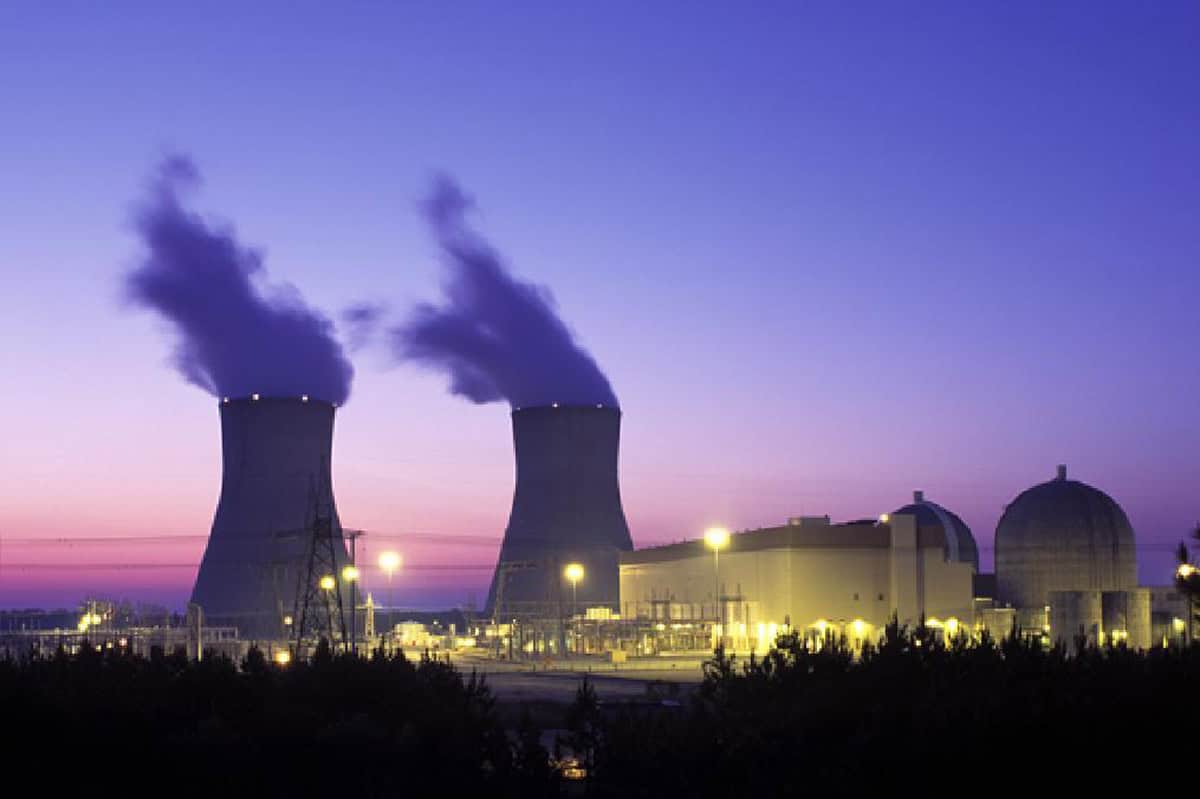
When I started my physics degree, I knew it could open the door to a range of career opportunities, but I wasn’t sure what path it would take me down. In the end, it was the optional modules that encouraged my interest in nuclear energy physics, steering me towards my current job as a nuclear safety engineer.
When I was looking at university degrees, I thought about studying chemical engineering, but my A-level physics teacher inspired me to consider physics instead. I’d always been fascinated with the subject, and enjoyed maths (and a challenge) too, so I thought why not give it a go.
I went on to study physics at the University of Liverpool, graduating in 2021. I absolutely loved the city and would highly recommend it to anyone considering physics – or any degree, for that matter. The campus is fantastic and Liverpool is an amazing place to be a student.
My undergraduate experience was incredibly rewarding. I met some of my closest friends and had countless memorable adventures. While the course was challenging at times, I have no regrets about choosing physics. I particularly enjoyed being able to pick specialist optional modules as it meant I could follow my interest in applied physics with topics such as nuclear power and medical physics.
In my final year, I started doing the obligatory job applications for those wanting to go into industry. But after receiving some rejections, I decided to explore an opportunity outside of science and ended up working for nearly a year in the charity sector as a Climate Action intern. There I undertook research projects related to decolonization in international development, and anti-racism and social justice, supporting the delivery of international development programmes.
While my time at Climate Action was rewarding and worthwhile, I wanted to move back into science and use my degree. Nuclear physics had been an area of interest for me since school, and my modules at university had encouraged that, so I turned my attention to the nuclear energy sector. Having worked for a charity, I was keen to find an organization whose values aligned with mine. Employee-owned engineering, management and development consultancy, Mott MacDonald, caught my eye, with its commitment to net zero, social outcomes and the UN’s Sustainable Development Goals.
I joined the the company’s three-year graduate scheme and, although I didn’t have any direct experience in safety, was offered a graduate nuclear safety position. It is a great role that ties in skills from my degree and my interest in nuclear while still presenting challenges and an opportunity to learn.
After two years at Mott MacDonald, I won Graduate of the Year at the UK Nuclear Skills Awards 2024. My colleagues had kindly nominated me, recognizing my dedication and drive, and the contribution I’d made to the organization. This opportunity was highly valuable for me and elevated my profile not only at Mott MacDonald but also within the sector. Then, after only two and half years in the graduate scheme, I was promoted to my current position of nuclear safety engineer.
My role focuses on developing nuclear safety cases – comprehensive sets of documents that assess and demonstrate the safety of nuclear facilities. With support from our wider team, the work involves analysing potential hazards and risks, outlining safety measures, and presenting a structured, evidence-based argument that the facility is safe for operation. I’ve worked on a variety of different projects including small modular reactors, nuclear medicine and flood alleviation schemes.
A typical day for me involves project meetings, writing safety reports, conducting hazard identification studies, and reviewing documents. A key aspect of the work is identifying, assessing and effectively controlling all project-related risks.
Beyond my technical role at Mott MacDonald, I am the programme director for our internal Women in Nuclear Network, and co-vice chair of the company’s Advancing Race and Culture Network. These positions allow me to contribute to a range of equality, diversity and inclusion (EDI) initiatives. Creating an inclusive environment is important to allow people the space to be authentically themselves, share and bring diverse perspectives and feel psychologically safe. This is a big driver for me – by supporting equity and equal opportunities, I am helping ensure others like me have role models in the sector.
Physics plays a crucial role in nuclear safety by providing the fundamental principles underlying nuclear processes. Studying nuclear physics at university has helped me understand and analyse reactor behaviour, radiation effects and potential hazards. This knowledge forms the basis for designing nuclear facility safety systems, for the protection of the workforce, environment and general public.
Throughout my degree, I also developed transferable skills such as analytical thinking, logical problem-solving and teamwork, all of which I apply daily in my role. As a safety-case engineer, I work as part of a team, and collaborate with specialists across fields, including process engineering, mechanical engineering and radioactive waste management. My ability to work effectively in teams and maintain strong interpersonal relationships has been key to success in my role.
I would encourage other physics students to explore a career in the nuclear industry
Applying my research and scientific report writing skills I developed at university, I can identify relevant information for safety-case updates, and present safety claims, arguments and evidence in a way that is understandable to a broad, non-specialist audience.
I also mentor and support more junior colleagues with various project and non-project related issues. Skills like critical thinking and the ability to tailor my communication style directly influence how I approach my work and support others.
I would encourage other physics students to explore a career in the nuclear industry. It offers a broad range of career paths, and the opportunity to contribute to some of the most diverse, exciting and challenging projects within the energy sector. You don’t need an engineering background to have a career in nuclear – there are many ways to contribute including beyond the technical route. As physicists we have a wide range of transferable skills, often more than we realize, making us highly adaptable and valuable in this sector.
It’s an incredible time to join the nuclear industry. With advancements like Sizewell C, small modular reactors, and cutting-edge medical nuclear-research facilities, there’s a wealth of diverse projects happening right now to get involved in. I hadn’t planned on a career in nuclear safety, but honestly, I’m really glad my path led this way. I am passionate about driving innovative nuclear solutions, and support progress towards reduced emissions and the global transition to net zero.
While I may be early on in my nuclear career, I have already worked on some interesting projects and met fantastic people. Now, I’m going through a structured training programme at Mott MacDonald to help me achieve chartership status with the Institute of Physics. I look forward to seeing what the future has to offer.
The post A physicist’s journey into nuclear energy appeared first on Physics World.
Particle therapy is an incredibly powerful cancer treatment. But it is also an incredibly expensive option that relies on massive, bulky accelerator systems. As such, in 2025 there were only 137 proton and carbon-ion therapy facilities in operation worldwide. So how can more people benefit?
Hoping to resolve this challenge, the LhARA collaboration is investigating a new take on particle therapy delivery: a laser-hybrid accelerator for radiobiological applications. The idea is to use laser-driven proton and ion beams to create a compact, high-throughput treatment facility to advance our understanding of cancer and its response to radiation (see: “A novel hybrid design”).
Last month, in the first of a series of CP4CT workshops, experts in the field came together at Imperial College London to discuss the potential advantages of laser-driven charged particles. The workshop aimed to examine the current status of particle therapy technology, assess how the unique properties of laser-driven beams could revolutionize particle therapy, and identify the key research needed to develop personalized cancer therapy with laser-driven ions.
“We want to lay the foundation for the transformation of ion beam therapy,” said Kenneth Long (Imperial College London/STFC), who co-organized the event together with Richard Amos (University College London). “We are aiming to engage with the communities that we will target when the technology is mature.”
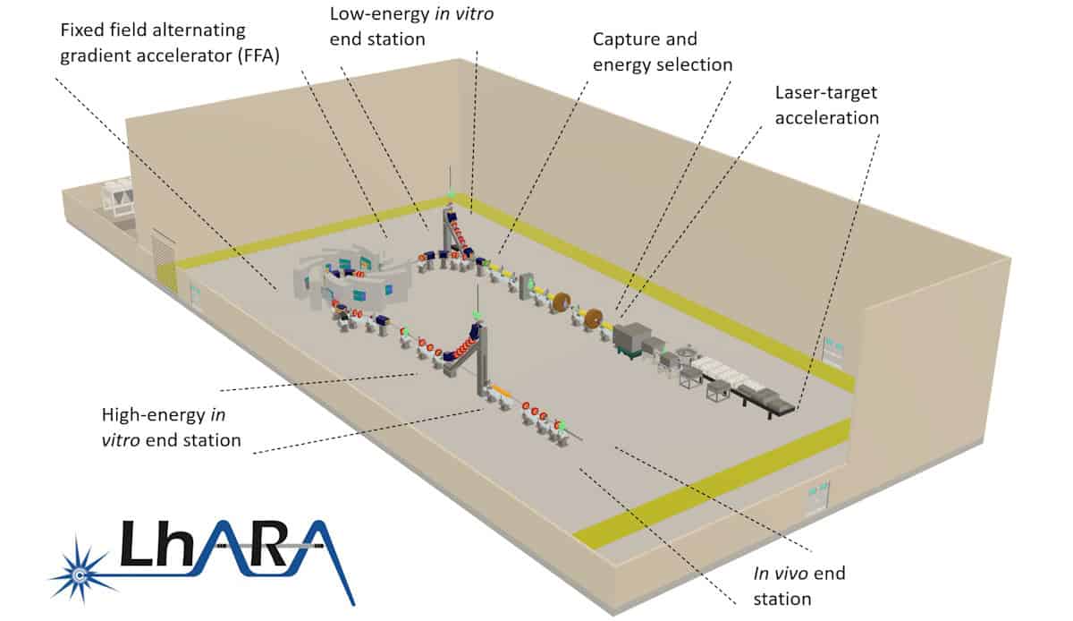
LhARA uses a high-power, fast-pulsed laser to create high-flux proton and ion beams with arbitrary spatial and time structures, such as bunches as short as 10 to 40 ns. The beams are captured and focused by a novel electron-plasma lens, and then accelerated using a fixed-field alternating gradient accelerator, to energies of 15–127 MeV for protons and 5–34 MeV/u for ion beams.
The LhARA team recently completed its conceptual design report for the proposed new accelerator facility and is now running radiobiology programmes to prove the feasibility of laser-driven hybrid acceleration, for both radiation biology and clinical studies.
The day’s first speaker, Alejandro Mazal (Centro de Protonterapia Quirónsalud) pointed out that despite huge clinical potential, only about 400,000 patients have been treated with proton therapy to date (and 65,000 with carbon ions), with a typical saturation of about 250 patients per year per treatment room. To increase this throughput, factors such as image guidance, adaptive tools, uptime and modularity for upgrades could prove vital.
Mazal cited some development priorities to address, including cost control, vendor robustness, system reliability and throughput optimization. It’s also vital to consider biological modulation techniques, integration into hospitals and generation of clinical evidence. “We used to say that randomized trials are not ethical with particle therapy but this is not always true, evidence must guide expansion,” he said.
Mazal emphasized that technology itself is not the endpoint, but that specifications must be driven by clinical benefit. “The goal is to be transformative, but only when we can measure a clinical value,” he explained.
Sandro Rossi (CNAO) then presented an update on the latest developments at the National Centre of Oncological Hadronotherapy (CNAO) in Italy. Since starting clinical treatments in 2011, the facility has now treated over 6000 patients – roughly half with protons and half with carbon ions. He noted that for some of the most challenging tumours, CNAO’s particle therapy delivered considerably better local tumour control than achieved by conventional X-ray treatments.
CNAO is also a research facility, currently hosting 17 funded research projects and seven active clinical trials. Looking forward, an expansion project will see the centre commission an additional proton therapy gantry, introduce boron neutron capture therapy (BNCT) and install an upright positioning system (from Leo Cancer Care) in one of the treatment rooms.
In parallel with the development of laser-based accelerators, researchers are investigating various radiobiological modulation strategies that could enhance the impact of particle therapy. The workshop examined three such options: proton minibeams, FLASH irradiation and combination with immunotherapies.
Minibeam therapy uses an array of submillimetre-sized radiation beams to deliver a pattern of alternating high-dose peaks and low-dose valleys. This spatially fractionated dose greatly reduces treatment toxicity while providing excellent tumour control, as demonstrated in extensive preclinical experiments.
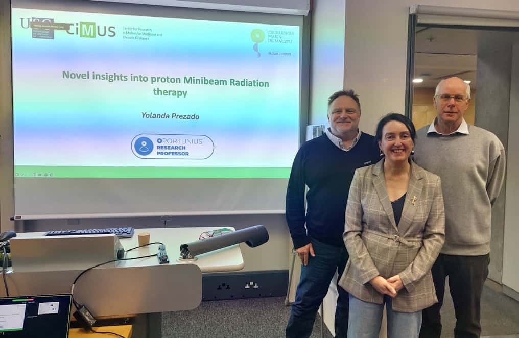
The first patient treatments (using X-ray minibeams) took place in 2024, and clinical investigations on proton minibeams are just starting, explained Yolanda Prezado (CiMUS). Recent studies revealed that minibeams induce a favourable immune response, with high T cell infiltration, vascular renormalization and reduced hypoxia dependence. Further evaluation is essential to explore the underlying radiobiological mechanisms, but Prezado noted that existing accelerators are limited in their ability to modulate treatment beams.
“It would be really interesting to have a system where we can flexibly vary all of the parameters to understand all of these techniques; LhARA could be a very interesting facility for this,” she suggested.
As for the second option, FLASH therapy, this is an emerging treatment approach in which radiation delivery at ultrahigh dose rates reduces normal tissue damage while effectively killing cancer cells. But how the FLASH effect works, and how to optimize this approach, remain key questions.
Joao Seco (DKFZ) presented a novel interpretation of FLASH, focusing on radiation chemistry and emphasizing the role of H2O2 generation in the FLASH process. Production of H2O2, a key molecule in cell damage, depends on the activity of a particular enzyme called superoxide dismutase 1 (SOD1). Seco hypothesized that inhibiting SOD1 could control H2O2 production and thus control cellular damage, effectively mimicking the FLASH effect.
“Forget radiation biology, we are missing a key component: redox chemistry,” he said. “If we know the redox chemistry, we can predict the response before we give radiotherapy.”
Marco Durante (GSI) suggested that the most urgent challenge for radiotherapy may be to combine it with immunotherapy, noting that charged particle beams offer both physical and biological advantages to achieve this. Citing various trials of combined immunotherapy and X-ray-based radiotherapy for cancer treatment, he showed some impressive examples of the benefit of the combination, but also cases with negative results.
“The question to understand is why doesn’t it always work,” he explained, suggesting that this may be due to the timing and sequencing of the two therapies, the fractionation scheme or biological factors. But perhaps a more promising approach would be to combine immunotherapy with particle therapy, he said, sharing examples where immunotherapy plus carbon-ions had better clinical outcomes than combinations with X-ray radiotherapy.
This superior outcome may arise from the various biological advantages of high-LET irradiation. Alongside, the lower integral dose from particle therapy compared with X-rays results in less lymphopenia (a low level of white blood cells), which is indicative of improved prognosis.
“Pre-clinical studies are essential to address timing and sequencing,” he concluded. “We also need more clinical trials to determine the impact of physical and biological properties of charged particles in radioimmunotherapy.”
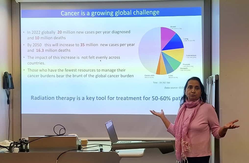
Manjit Dosanjh (University of Oxford) discussed the continuing need to increase global access to radiotherapy, noting that while radiotherapy is a key tool for over 50% of cancer patients, not all countries have access to sufficient treatment systems, nor to the expert personnel needed to run them.
Across Africa, for instance, there is just one linac per 3.5 million people, in stark contrast to the one per 86, 000 people in the US. Many European countries also lack sufficient quality or quantity of radiotherapy facilities – a disparity that’s mirrored in terms of access to CT scanners, oncologists and medical physicists, which must be addressed in tandem. “If we could improve imaging, treatments and care quality, we could prevent 9.6 million deaths per year worldwide,” Dosanjh said.
She described some initiatives designed to encourage collaboration and increase access, including ENLIGHT, the European Network for Light Ion Hadron Therapy. Launched in 2002 at CERN, ENLIGHT brings together clinicians, physicists, biologists and engineers working within particle therapy to develop new technologies and provide training, education and access to beams to move the field forward.
More recently, the STELLA (smart technologies to extend lives with linear accelerators) project was established to create a cost-effective, robust radiotherapy linac with lower staff requirements and maximal uptime. A global collaboration, STELLA aims to expand access to high-quality cancer treatment for all patients via innovative transformation of the treatment system, as well as providing training, education and mentoring.
Dosanjh also introduced SAPPHIRE, a UK-led initiative that partners with institutions in Ghana and South Africa to strengthen radiotherapy services across Africa. She stressed that improving access to radiotherapy is a big challenge that can only be achieved by building really good collaborations. “Collaboration is the invisible force that makes the impossible possible,” she said.
Konrad Nesteruk (Harvard) continued the theme of democratizing particle therapy, noting that advancement of beam technologies calls for innovations in space (the facility size), time (both irradiation and total treatment time) and dose (via techniques such as FLASH, proton arc and minibeams). All of these factors interact to create a multidimensional optimization problem, he explained.
The final speaker in this session, Rock Mackie (University of Wisconsin) examined how to translate innovative radiotherapy technology into clinical practice. Academia is the source of breakthrough ideas, he said, but most R&D is funded and refined by companies. And forming a company involves a series of key tasks: identifying an important problem; developing a technical solution; patenting it; customer testing; and procuring investment. If this final stage doesn’t happen, Mackie remarked, it wasn’t an important enough problem.
In particle therapy, the main problems are size and cost limiting patient access, a lack of effective imaging solutions and the fact that the gain in therapeutic ratio does not compensate for increased costs. Aiming to solve these problems, Mackie co-founded Leo Cancer Care in 2018 to commercialize an upright patient positioning system and CT scanner. This approach enables a proton therapy machine to fit into a photon vault, as well as easing patient positioning, thus reducing installation costs while simultaneously increasing throughput.
Mackie applied this startup scenario to LhARA. Here, the problem to solve is achieving high-energy, multi-ion, high-intensity beams for radiotherapy, FLASH, spatial fractionation and proton imaging. The solution is the development of a low-cost particle accelerator that meets all of these needs and fits in a single-storey vault. He also emphasized the importance of consulting with as many potential customers as time permits before defining specifications.
“The most important problem is finding a big enough problem to solve,” he concluded. “It will find a market if the product is less costly, works better and is easier to use.”
Alexander Gerbershagen (PARTREC) told delegates about PARTREC, the particle therapy research centre at the University Medical Center Groningen. The facility’s superconducting accelerator, AGOR, provides protons with energies up to 190 MeV, as well as ion beams of all elements up to xenon. Ongoing projects at PARTREC include: developing glioblastoma treatments using boron proton capture therapy (NuCapCure); production of terbium isotopes for theranostics; image-guided pharmacotherapy using photon-activated drugs; and real-time in vivo verification of proton therapy dose.
The day closed with a look at the potential of LhARA as an international research facility. Kenneth Long emphasized the importance of investigating how ionizing radiation interacts with tissue, in vivo and in vitro, while considering all of the factors that may impact outcome. This includes time and space domains, different ion species and energies, and combinations with chemo- and immunotherapy. “If one flexible beam facility can do all that, it’s a substantial opportunity for a step change in understanding,” he said.
Long presented some initial cell irradiations using laser-driven beams at the SCAPA research centre in Strathclyde, and noted that component optimization is also underway in Swansea. He also shared designs for the envisaged research facility, with various in vivo and in vitro end-stations and robotic automation to move experiments around. “We have written a mission statement, now our business is to execute that programme,” he concluded.
The post A glimpse into the future of particle therapy appeared first on Physics World.

NASA’s Commercial Crew Program was supposed to be the template: services-based procurement, private ownership of hardware and competition between providers. Yet NASA has now formally designated Boeing’s 2024 Starliner crewed test flight as a Type A mishap — its most serious category — and leadership has been explicit that the most troubling failure was not […]
The post Starliner and Artemis: commercial label vs. commercial discipline appeared first on SpaceNews.

Denver-based Lux Aeterna has secured $10 million in seed funding to develop a reusable satellite designed to survive atmospheric reentry and fly again with new payloads, starting with a demonstration flight slated for early 2027.
The post Lux Aeterna raises $10 million ahead of 2027 reusable satellite demo appeared first on SpaceNews.

Chinese launch startup Landspace says it has completed a long-duration full-system hot-fire test of its new 220-ton-class methane rocket engine for new-generation launchers.
The post Landspace tests 220-ton methane engine for future heavy-lift launchers appeared first on SpaceNews.

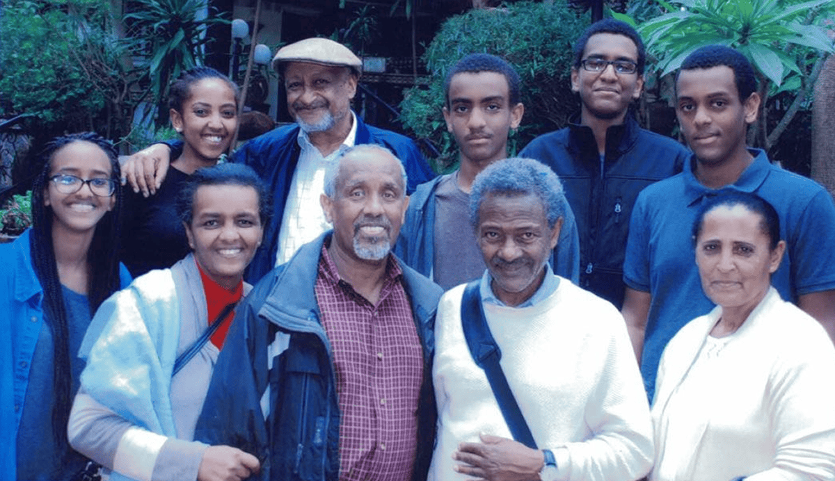
Mulugeta Bekele paid a heavy price for remaining in Ethiopia in the 1970s and 1980s. While many other academics had fled their homeland to avoid being targeted by its military rulers, Mulugeta did not. He stayed to teach physics, almost single-handedly keeping it alive in the country. But Mulugeta was arrested and brutally tortured by members of the Derg, Ethiopia’s ruling military junta. “I still have scars,” he says when we meet at his tiny, second-floor office at Addis Ababa University (AAU) in January 2026.
Gentle and softly-spoken, Mulugeta, 79, is formally retired but still active as a research physicist. In 2012 his efforts led to him being awarded the Sakharov prize by the American Physical Society (APS) “for his tireless efforts in defence of human rights and freedom of expression and education anywhere in the world, and for inspiring students, colleagues and others to do the same”.
Mulugeta was born in 1947 near Asela, a small town south of Ethiopia’s capital Addis Ababa. The district had only a single secondary school that depended on volunteer teachers from other countries. One was a US Peace Corps volunteer named Ronald Lee, who taught history, maths and science for two years. Mulugeta recalls Lee as a dramatic and inventive teacher, who would climb trees in physics classes to demonstrate the actions of pulleys and hold special after-school calculus classes for advanced students.
Mulugeta and other Asela students were entranced. So when he entered AAU – then called Haile Selassie 1 University – in 1965, Mulugeta declared he wanted to study both mathematics and physics. Impossible, he was informed; he could do one or the other but not both. “I told myself that if I choose mathematics I will miss physics,” Mulugeta says. “But if I do physics, I will be continually engaged with mathematics.” Physics it was.
At the end of his third year, Mulugeta’s studies appeared in doubt. The university’s only physics teacher was an American named Ennis Pilcher, who was about to return to Union College in Schenectady, New York, after spending a year in Addis on a fellowship from the Fulbright Program. Pilcher, though, managed to convince Union to support Mulugeta so he could travel to the US and study physics there for his final year.
As I talk to Mulugeta, he pulls a dusty book off his shelf. “This was given to me by Pilcher,” he says, pointing to Walter Meyerhof’s classic undergraduate textbook Elements of Nuclear Physics. Mulugeta turns to the inside of the front cover and proudly shows me the inscription: “Mulugeta Bekele, Union College. Schenectady, 1969–1970”.
When Mulugeta returned to AAU in the summer of 1970, he was awarded a BSc in physics. He then received a grant from the US Agency for International Development (USAID) to attend the University of Maryland for a master’s degree. After two more years in the US, Mulugeta returned to Addis Ababa in 1973. As an accomplished researcher and teacher, he was made department chair and began to expand the physics programme at the university.
It was a time when political turmoil was upending Ethiopia, as well as the lives of Mulugeta and many other academics. For centuries the country had been ruled by a dynasty whose present emperor was Haile Selassie. Having come to the throne in 1930, he had tried to reform Ethiopia by bringing it into the League of Nations, drawing up a constitution, and taking measures to abolish slavery.
When fascist Italy invaded Ethiopia in May 1935, Selassie left, spending six years in exile in the UK during the Italian occupation of the country. He returned as emperor in 1941 after British and Ethiopian forces recaptured Addis Ababa. But famine, unemployment and corruption, as well as a brief unsuccessful coup attempt, undermined his rule and made him unexpectedly vulnerable.
While in Maryland, Mulugeta and other Ethiopian students in the US started supporting the Ethiopian People’s Revolutionary Party (EPRP) – a pro-democracy group that sought to build popular momentum against the monarchy. In February 1974 Selassie was deposed by the Derg – a repressive military junta named after the word for “committee” in Amharic, the most widely spoken language in Ethiopia. Selassie was assassinated the following year.
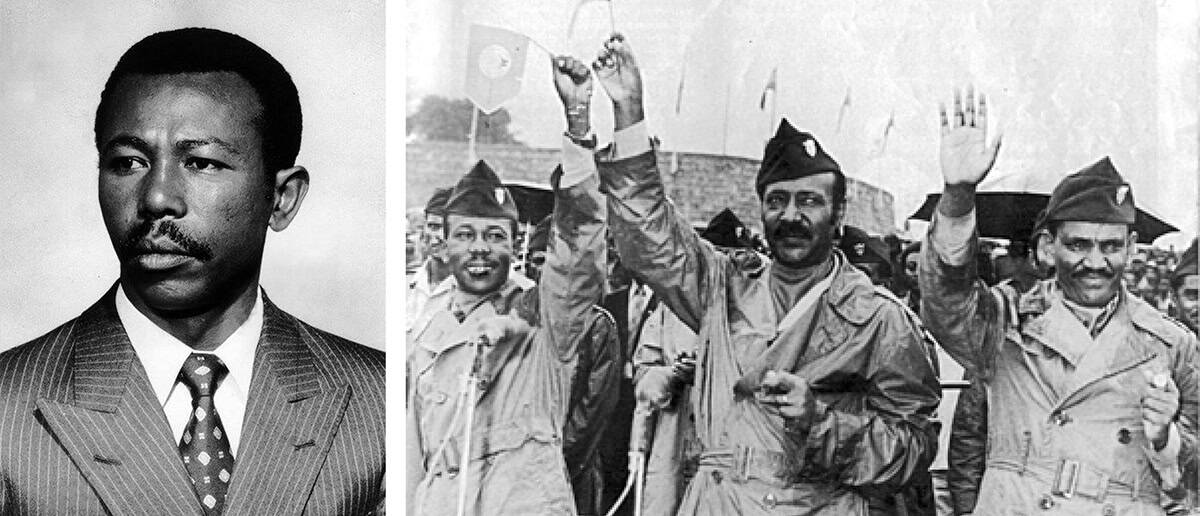
Led by an army officer named Mengistu Haile Mariam, the Derg’s radical totalitarianism was in sharp contrast to the student-led EPRP’s efforts and its agenda included seizing property from landowners. Mulugeta’s family lost all its land, and his father was killed fighting the Derg. “Land ownership was still inequitable,” Mulugeta remarks ruefully, “only the landlords changed.”
In September 1976 the EPRP tried, unsuccessfully, to assassinate Mengistu. The following February, on becoming chairman of Derg – and therefore head of state – Mengistu began ruthlessly to crush any opposition, particularly the EPRP, in what he himself called the “Red terror” campaign of political suppression. About half a million people in Ethiopia were killed.
“It was a police state,” recalls Solomon Bililign, Mulugeta’s then graduate assistant, now a professor of atomic and molecular physics at North Carolina Agricultural and Technical State University. “The police didn’t need any reason to arrest you. They would arrest people openly in the streets, break into homes, and left people dead in roads and parks. Many were tortured; others simply disappeared.”
Mulugeta himself was a target. In the summer of 1977, a policeman showed up at his office with an informant. Mulugeta was arrested and imprisoned for his role in helping to organize anti-Derg activities, as was Bililign. Mulugeta still recalls exactly how long he was jailed for: “Eight months and 20 days”.
After his release, Mulugeta knew it would be unsafe to stay in Addis and lived in hiding for several months. So he devised a plan to travel 500 km north to a holdout region not controlled by the Derg. However, while using a fake ID to pass through checkpoints to reach a compatriot, he was betrayed again, captured, and taken back to Addis.
Mulugeta was savagely tortured using a method that the Derg meted out on thousands of other prisoners.
En route to Addis, he managed to steal back the fake ID that he’d been using from the pocket of the policeman travelling with him. He then tore it up to shield the identity of his compatriot, and tossed the pieces into a toilet. But the policeman noticed and retrieved the pieces. Mulugeta was then savagely tortured using a method that the Derg meted out on thousands of other prisoners. His arms and legs were tied around a pole, and he was hung in the foetal position between two chairs, upside down. His feet were then beaten until he could no longer walk.
Mulugeta was sent to Maekelawi, an infamous jail in Addis, in which up to 70 prisoners could be jammed in rooms each barely four metres long and four metres wide. Inmates were tortured without warning, could not have visitors, never had trials, were denied books and paper, and at night heard screams from periodic executions. Mulugeta helped those who were beaten by tending to their wounds.
“People who knew him in prison told me that his mental strength helped all of them endure,” remembers Mesfin Tsige, an undergraduate student of Mulugeta at the time, who is now a polymer physicist at the University of Akron in Ohio. Despite the awful conditions, Mulugeta managed to continue working on physics by surreptitiously taking paper from the foil linings of cigarette packets to compose problems.
Another prisoner was Nebiy Mekonnen, a chemistry student of Mulugeta. Later a gifted artist, translator and newspaper editor, Mekonnen began translating the US writer Margaret Mitchell’s classic 1936 book Gone with the Wind into Amharic. It was the one book that the Maekelawi prisoners had in their hands, having retrieved it from the possessions of someone who had been executed.
Surreptitiously writing his translation onto the foil linings of cigarette packets, Mekonnen would read passages to fellow prisoners in the evening for what passed for entertainment. Mekonnen’s translation of Mitchell’s almost 1000-page book was recorded onto 3000 of the linings, which were then smuggled out of the prison stuffed in tobacco pouches and published years later.
Gone with the Wind might seem a strange choice to translate, but as Mulugeta reminds me: “It was the only book we had at the time”. More smuggled books did eventually arrive at the prison, but Gone with the Wind, which describes life in a war-torn country, has several passages that resonated with prisoners. One was: “In the end what will happen will be what has happened whenever a civilization breaks up. The people with brains and courage come through and the ones who haven’t are winnowed out.”
In 1982, Mulugeta was moved to Kerchele, another prison. There, as at Maekelawi, inmates were forced to listen to Mengistu’s pompous speeches on radio and TV. During one Mengistu pontificated that he would turn prisons into places of education. A clever inmate, knowing that the prison wardens were also cowering in terror, proposed that Kerchele establish a school with the prisoners as teachers.
The wardens found this a great idea, not least because it let them show off their loyalty to Mengistu. The Kerchele prisoners were promptly put to work erecting a schoolhouse of half a dozen rooms out of asbestos slabs. Unlike schools in the rest of Ethiopia, the Kerchele prison school was not short of teachers, as the prisoners included a wide range of professionals, such as architects, scientists and engineers.
Students included prison guards and their families, along with numerous inmates who had been jailed for non-political reasons. Mulugeta and Bililign taught physics. “It was therapy for us,” Bililign says – and the school was soon known as one of the best in Ethiopia.
When I ask Mulugeta how he maintained his interest in physics in jail, despite being locked up for so many years, he becomes animated.
When I ask Mulugeta how he maintained his interest in physics in jail, despite being locked up for so many years, he becomes animated. “In those days, prisons were full of ideas,” he smiles. “We were university students, university teachers. We had a cause. It was exciting. Intellectually, we flourished.”
In the summer of 1985 Mulugeta was released. Many colleagues were not. “They were given release papers and as they left the building, one by one, they were strangled. I had a tenth-grade student who was one of the best; he didn’t make it. There were plenty of stories like this.” Mulugeta pauses. “Somehow we survived. But not them.”
Mulugeta returned to the university, now renamed from Haile Selassie University to Addis Ababa University, and started teaching physics full time. As the Derg was in full control no opposition was possible except in outer regions of Ethiopia. In summer 1991, after Mulugeta had taught physics for another six years, political turmoil erupted yet again.
Mengistu was overthrown that May by a political coalition representing pro-democracy groups from five of Ethiopia’s ethnic regions, the Ethiopian People’s Revolutionary Democratic Front (EPRDF). But ethnic tensions rose and human rights violations continued. “Even though the Derg was overthrown,” Mulugeta recalls, “we knew we were entering another dark age.”
In the same year Mulugeta was put in touch with a Swedish programme seeking to build networks of scientists across countries in the southern hemisphere. Mulugeta knew a physicist from Bangalore, India, who had visited Addis twice as an examiner for his master’s programme and arranged to work with him for his PhD.
That July, Mulugeta married Malefia, who worked in the university’s registrar office, and the two left for Bangalore. As a wedding present, his student Mekonnen painted a picture of two hands coming together, each with a ring on a finger, against a black Sun in the background. “Two rings, in the time of a dark sun” Mekonnen’s caption read, “Happy marriage!” Mulugeta still has the painting.
Mulugeta thrived in Bangalore. Here, he was finally able to combine his two loves, physics and maths, studying statistical physics and stochastic processes and applying them to issues in non-equilibrium thermodynamics. He has worked in that field ever since. He received his PhD in 1998 from the Indian Institute of Science in Bangalore and returned to Addis once more to teach.
Shortly after Mulugeta’s return from Bangalore to Ethiopia in August 1998, some of his former students formed the Ethiopian Physical Society, electing him as its first president. Other students of his who had taken positions in the US created the Ethiopian Physical Society of North America (EPSNA), formally established in 2008. Bililign organized and convened its first meeting.
In 2007, Philip Taylor, a soft-condensed-matter physicist from Case Western Reserve University in the US, who had been Tsige’s PhD supervisor, heard the story of Mulugeta’s imprisonment. Astonished, he spearheaded the successful 2012 application for Mulugeta to receive the APS’s Sakharov prize, which is given every two years to physicists who have displayed “outstanding leadership and achievements of scientists in upholding human rights”.
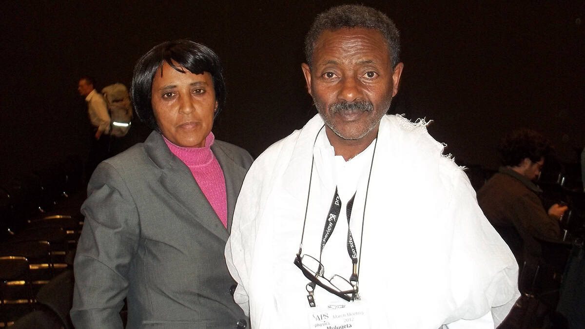
Unsure that he would receive travel funds to attend a special award ceremony at that year’s APS March meeting in Boston, the EPSNA raised money for Mulugeta and his wife to attend. Jetlagged, worn out by the cold, and somewhat overwhelmed by the attention, Mulugeta could not be found as the ceremony began. EPSNA members tracked him down to his hotel room, where he was dressing in traditional Ethiopian clothes for the occasion – all white from head to toe, including shoes.
In recent years, Mulugeta has continued to teach and collaborate with students and former students, publishing in a wide range of journals, as well as helping out with the Ethiopian Physical Society. But while I was in Ethiopia to talk to Mulugeta at the start of 2026, the Trump administration curtailed immigrant visas from Ethiopia and almost half of all nations in Africa supposedly in an attempt to “protect the security of the United States”. A few months before, it had imposed a $100,000 fee on work visas, all but preventing US universities from hiring non-US citizens. It killed the USAID programme that had once sent Mulugeta to the US for his master’s degree.
The Trump administration has also withdrawn the US from international scientific organizations, conventions and panels, and has gutted the most important US scientific agencies. These and other measures are destroying the networks of international physics collaborations of the kind that Mulugeta both promoted and benefited from – networks that nurture education, careers and knowledge.
“We are not yet in good hands,” Mulugeta warns me as I start to leave. “We are,” he says, “still under the dark Sun.”
The post Mulugeta Bekele: the jailed and tortured scientist who kept Ethiopian physics alive appeared first on Physics World.
