With six additional satellites launching in May and continued expansion later this year, the EarthDaily Constellation will enter commercial operations in Summer 2026, delivering daily, consistent global coverage.
If the United States wants to defend the homeland against the next generation of missile and aerial threats, hardware alone will not save us. Sensors, radars and interceptors are necessary but no longer sufficient. The decisive advantage for Golden Dome for America will come from software and the ability to integrate, test, adapt and fight […]
A newly identified metallic material that conducts heat nearly three times better than copper could redefine thermal management in electronics. The material, which is known as theta-phase tantalum nitride (θ-TaN), has a thermal conductivity comparable to low-grade diamond, and its discoverers at the University of California Los Angeles (UCLA), US say it breaks a record on heat transport in metals that had held for more than 100 years.
Semiconductors and insulators mainly carry heat via vibrations, or phonons, in their crystalline lattices. A notable example is boron arsenide, a semiconductor that the UCLA researchers previously identified as also having a high thermal conductivity. Conventional metals, in contrast, mainly transport heat via the flow of electrons, which are strongly scattered by lattice vibrations.
Heat transport in θ-TaN combines aspects of both mechanisms. Although the material retains a metal-like electronic structure, study leader Yongjie Hu explains that its heat transport is phonon-dominated. Hu and his UCLA colleagues attribute this behaviour to the material’s unusual crystal structure, which features tantalum atoms interspersed with nitrogen atoms in a hexagonal pattern. Such an arrangement suppresses both electron–phonon and phonon–phonon scattering, they say.
Century-old upper limit for metallic heat transport
Materials with high thermal conductivity are vital in electronic devices because they remove excess heat that would otherwise impair the devices’ performance. Among metals, copper has long been the material of choice for thermal management thanks to its relative abundance and its thermal conductivity of around 400 Wm−1 K−1, which is higher than any other pure metal apart from silver.
Recent theoretical studies, however, had suggested that some metallic-like materials could break this record. θ-TaN, a metastable transition metal nitride, was among the most promising contenders, but it proved hard to study because high-quality samples were previously unavailable.
Highest thermal conductivity reported for a metallic material to date
Hu and colleagues overcame this problem using a flux-assisted metathesis reaction. This technique removed the need for the high pressures and temperatures required to make pure samples of the material using conventional techniques.
The team’s high-resolution structural measurements revealed that the as-synthesized θ-TaN crystals had smooth, clean surfaces and ranged in size from 10 to 100 μm. The researchers also used a variety of techniques, including electron diffraction, Raman spectroscopy, single-crystal X-ray diffraction, high-resolution transmission electron microscopy and electron energy loss spectroscopy to confirm that the samples contained single crystals.
The researchers then turned their attention to measuring the thermal conductivity of the θ-TaN crystals. They did this using an ultrafast optical pump-probe technique based on time-domain thermoreflectance, a standard approach that had already been used to measure the thermal conductivity of high-thermal-conductivity materials such as diamond, boron phosphide, boron nitride and metals.
Hu and colleagues made their measurements at temperatures between 150 and 600 K. At room temperature, the thermal conductivity of the θ-TaN crystals was 1100 Wm−1 K−1. “This represents the highest value reported for any metallic materials to date,” Hu says.
The researchers also found that the thermal conductivity remained uniformly high across an entire crystal. H says this reflects the samples’ high crystallinity, and it also confirms that the measured ultrahigh thermal conductivity originates from intrinsic lattice behaviour, in agreement with first-principles predictions.
Another interesting finding is that while θ-TaN has a metallic electronic structure, its thermal conductivity decreased with increasing temperature. This behaviour contrasts with the weak temperature dependence typically observed in conventional metals, in which heat transport is dominated by electrons and is limited by electron-phonon interactions.
Applications in technologies limited by heat
As well as cooling microelectronics, the researchers say the discovery could have applications in other technologies that are increasingly limited by heat. These include AI data centres, aerospace systems and emerging quantum platforms.
The UCLA team, which reports its work in Science, now plans to explore scalable ways of integrating θ-TaN into device-relevant platforms, including thin films and interfaces for microelectronics. They also aim to identify other candidate materials with lattice and electronic dynamics that could allow for similarly efficient heat transport.
02.19.2026 DURANGO, Colo. — Agile Space Industries, a leading provider of in-space chemical propulsion, today announced their Series A equity financing round. The round was led by Caruso Ventures and […]
Japanese lunar company ispace said work on a new engine for its lunar landers is facing delays and that it is keeping open the option of switching engines.
The Defense Innovation Unit plans to select companies to field and operate spacecraft before transferring them to government control within three years
A new report finds that of 154 specific claims about how AI will benefit the climate, just a quarter cited academic research. A third included no evidence at all.
With the final GPS III satellite scheduled to launch in March, the United States is completing the most significant upgrade to its positioning, navigation, and timing (PNT) infrastructure in more than a decade. GPS III delivers improved accuracy, stronger signals and enhanced anti-jam capabilities for military users. By any technical measure, it is a better […]
Synthetic materials such as plastics are designed to be durable and water resistant. But the processing required to achieve these properties results in a lack of biodegradability, leading to an accumulation of plastic pollution that affects both the environment and human health. Researchers at the Institute for Bioengineering of Catalonia (IBEC) are developing a possible replacement for plastics: a novel biomaterial based on chitin, the second most abundant natural polymer on Earth.
“Every year, nature produces on the order of 1011 tonnes of chitin, roughly equivalent to more than three centuries of today’s global plastic production,” says study leader Javier G Fernández. “Chitin and [its derivative] chitosan are the ultimate natural engineering polymers. In nature, variations of this material produce stiff insect wings enabling flight, elastic joints enabling extraordinary jumping in grasshoppers, and armour-like protective exoskeletons in lobsters or clams.”
But while biomaterials provide a more environmentally friendly alternative to conventional plastics, most biological materials weaken when exposed to water. In this latest work, Fernández and first author Akshayakumar Kompa took inspiration from nature and developed a new biomaterial that increases its strength when in contact with water, while maintaining its natural biodegradability.
Metal matters
In the exoskeletons of insects and crustaceans, chitin it is secreted in a gel-like form into water and then transitions into a hard structure. Following a chance observation that removing zinc from a sandworm’s fangs caused them to soften in water, Kompa and Fernández investigated whether adding a different transition metal, nickel, to chitosan could have the opposite effect.
By mixing nickel chloride solution (at concentrations from 0.6 to 1.4 M) with dispersions of chitosan extracted from discarded shrimp shells, the researchers entrapped varying amounts of nickel within the chitosan structure. Fourier-transform infrared spectra of resulting chitosan films revealed the presence of nickel ions, which form weak hydrogen bonds with water molecules and increase the biomaterial’s capacity to bond with water.
“In our films, water molecules form reversible bridges between polymer chains through weak interactions that can rapidly break and reform under load,” Fernández explains. “That fast reconfiguration is what gives the material high strength and toughness under wet conditions: essentially a built-in, stress-activated ‘self-rearrangement’ mechanism. Nickel ions act as stabilizing anchors for these water-mediated bridges, enabling more and longer-range connections and making inter-chain connectivity more robust”.
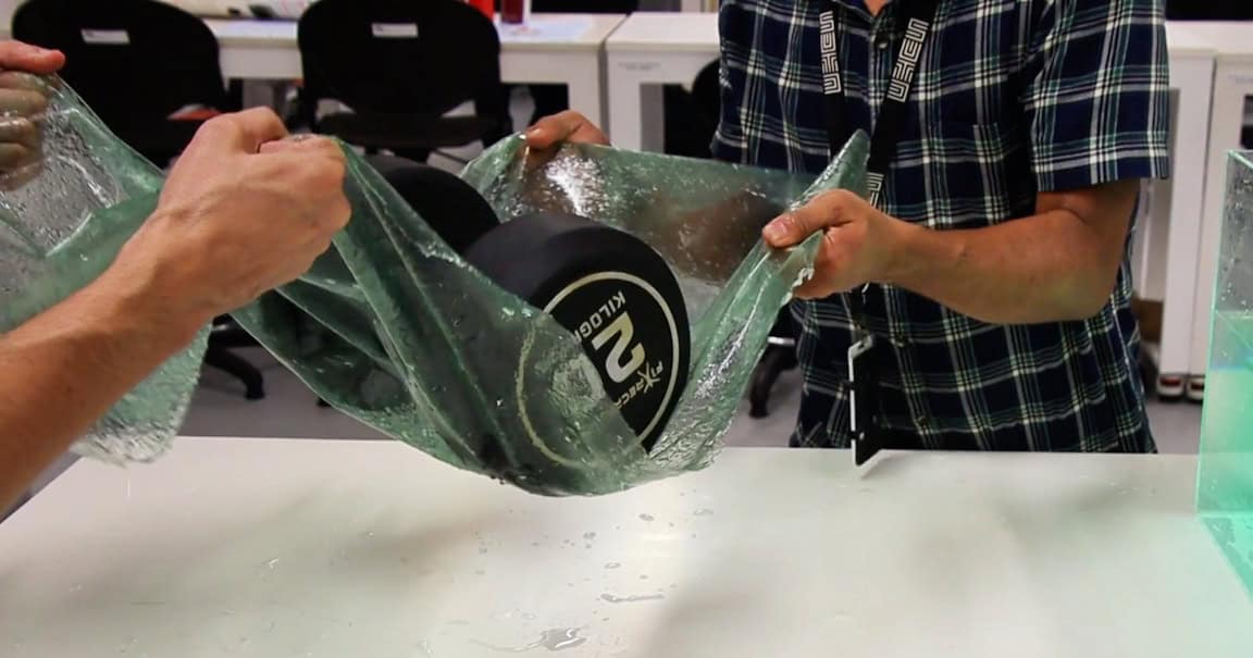
The nickel-doped chitosan samples had tensile strengths of between 30 and 40 MPa, similar to that of standard plastics. Adding low concentrations of nickel did not significantly impact the mechanical properties of the films. Concentrations of 1 M or more, however, preserved the material’s strength while increasing its toughness (the ability to stretch before breaking) – a key goal in the field of structural materials and a feature unique to biological composites.
Increased strength Testing a nickel-doped chitosan film using a 20 kg dumbbell. (Courtesy: Institute for Bioengineering of Catalonia)
Upon immersion in water, the nickel-doped films exhibited greater tensile strength, increasing from 36.12±2.21 MPa when dry to 53.01±1.68 MPa, moving into the range of higher-performance engineering plastics. In particular, samples created from an optimal 0.8 M nickel concentration almost doubled in strength when wet (and were used for the remainder of the team’s experiments).
Scaling production
The manufacturing process involves an initial immersion in water, followed by drying for 24 h and then re-wetting. During the first immersion, any nickel ions that are not incorporated into the material’s functional bridging network are released into the water, ensuring that nickel is present only where it is structurally useful.
The researchers developed a zero-waste production cycle in which this water is used as a primary component for fabricating the next object. “The expelled nickel is recovered and used to make the next batch of material, so the process operates at essentially 100% nickel utilization across batches,” says Fernández.
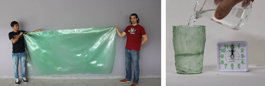
Zero waste production The team created structures including a 3 m2 nickel-doped chitosan film and a cup that can retain water as effectively as common plastics. (Courtesy: Institute for Bioengineering of Catalonia)
They used this process to produce various nickel-doped chitosan objects, including watertight containers and a 1 m2 film that could support a 20 kg weight after 24 h of water immersion. They also created a 244 x 122 cm film with similar mechanical behaviour to the smaller samples, demonstrating the potential for rapid scaling to ecologically relevant scales. A standard half-life test revealed that after approximately four months buried in garden soil, half of the material had biodegraded.
The researchers suggest that the biomaterial’s first real-world use may be in sectors such as agriculture and fishing that require strong, water-compatible and ultimately biodegradable materials, likely for packaging, coatings and other water-exposed applications. Both nickel and chitosan are already employed within biomedicine, making medicine another possible target, although any new medical product will require additional regulatory and performance validation.
The team is currently setting up a 1000 m2 lab facility in Barcelona, scheduled to open in 2028, for academia–industry collaborations in sustainable bioengineering research. Fernández suggests that we are moving towards a “biomaterial age”, defined by the ability to “control, integrate, and broadly use biomaterials and biological principles within engineering applications”.
“Over the last 20 years, working on bioinspired manufacturing, we have been able to produce the largest bioprinted objects in the world, demonstrated pathways for resource-secure and sustainable production in urban environments, and even explored how these approaches can support interplanetary colonization,” he tells Physics World. “Now we are achieving material properties that were considered out of reach by designing the material to work with its environment, rather than isolating itself from it.”
A new SpaceX initiative to provide space traffic coordination services has attracted attention and praise in part because of the conditions it places on users of it.
A long-awaited cap on liability for U.K. launch operators came into force Feb. 18, aiming to make the country’s fledgling rocket sector more competitive as it struggles to get off the ground.
Electronics made from certain atomically thin materials can survive harsh radiation environments up to 100 times longer than traditional silicon-based devices. This finding, which comes from researchers at Fudan University in Shanghai, China, could bring significant benefits for satellites and other spacecraft, which are prone to damage from intense cosmic radiation.
Cosmic radiation consists of a mixture of heavy ions and cosmic rays, which are high-energy protons, electrons and atomic nuclei. The Earth’s magnetic field protects us from 99.9% of this ionizing radiation, and our atmosphere significantly attenuates the rest. Space-based electronics, however, have no such protection, and this radiation can damage or even destroy them.
Adding radiation shielding to spacecraft mitigates these harmful effects, but the extra weight and power consumption increases the spacecraft’s costs. “This conflicts with the requirements of future spacecraft, which call for lightweight and cost-effective architectures,” says team leader Peng Zhou, a physicist in Fudan’s College of Integrated Circuits and Micro-Nano Electronics. “Implementing radiation tolerant electronic circuits is therefore an important challenge and if we can find materials that are intrinsically robust to this radiation, we could incorporate these directly into the design of onboard electronic circuits.”
Promising transition-metal dichalcogenides
Previous research had suggested that 2D materials might fit the bill, with transistors based on transition-metal dichalcogenides appearing particularly promising. Within this family of materials, 2D molybdenum disulphide (MoS2) proved especially robust to irradiation-induced defects, and Zhou points out that its electrical, mechanical and thermal properties are also highly attractive for space applications.
The studies that revealed these advantages were, however, largely limited to simulations and ground-based experiments. This meant they were unable to fully replicate the complex and dynamic radiation fields such circuits would encounter under real space conditions.
Better than NMOS transistors
In their work, Zhou and colleagues set out to fill this gap. After growing monolayer 2D MoS2 using chemical vapour deposition, they used this material to fabricate field-effect transistors. They then exposed these transistors to 10 Mrad of gamma-ray irradiation and looked for changes to their structure using several techniques, including cross-sectional transmission electron microscopy (TEM) imaging and corresponding energy-dispersive spectroscopy (EDS) mapping.
These measurements indicated that the 2D MoS2 in the transistors was about 0.7 nm thick (typical for a monolayer structure) and showed no obvious signs of defects or damage. Subsequent Raman characterization on five sites within the MoS2 film confirmed the devices’ structural integrity.
The researchers then turned their attention to the transistors’ electrical properties. They found that even after irradiation, the transistors’ on-off ratios remained ultra-high, at about 108. They note that this is considerably better than a similarly-sized Si N-channel metal–oxide–semiconductor (NMOS) transistors fabricated through a CMOS process, for which the on-off ratio decreased by a factor of more than 4000 after the same 10 Mrad irradiation.
The team also found that MoS2 system consumes only about 49.9 mW per channel, making its power requirement at least five times lower than the NMOS one. This is important owing to the strict energy limitations and stringent power budgets of spacecraft, Zhou says.
Surviving the space environment
In their final experiment, the researchers tested their MoS2 structures on a spacecraft orbiting at an altitude of 517 km, similar to the low-Earth orbit of many communication satellites. These tests showed that the bit-error rate in data transmitted from the structures remained below 10-8 even after nine months of operation, which Zhou says indicates significant radiation and long-term stability. Indeed, based on test data, electronic devices made from these 2D materials could operate for 271 years in geosynchronous orbit – 100 times longer than conventional silicon electronics.
“The discovery of intrinsic radiation tolerance in atomically thin 2D materials, and the successful on-orbit validation of the atomic-layer semiconductor-based spaceborne radio-frequency communication system have opened a uniquely promising pathway for space electronics leveraging 2D materials,” Zhou says. “And their exceptionally long operational lifetimes and ultra-low power consumption establishes the unique competitiveness of 2D electronic systems in frontier space missions, such as deep-space exploration, high-Earth-orbit satellites and even interplanetary communications.”
The researchers are now working to optimize these structures by employing advanced fabrication processes and circuit designs. Their goal is to improve certain key performance parameters of spaceborne radio-frequency chips employed in inter-satellite and satellite-to-ground communications. “We also plan to develop an atomic-layer semiconductor-based radiation-tolerant computing platform, providing core technological support for future orbital data centres, highly autonomous satellites and deep-space probes,” Zhou tells Physics World.